


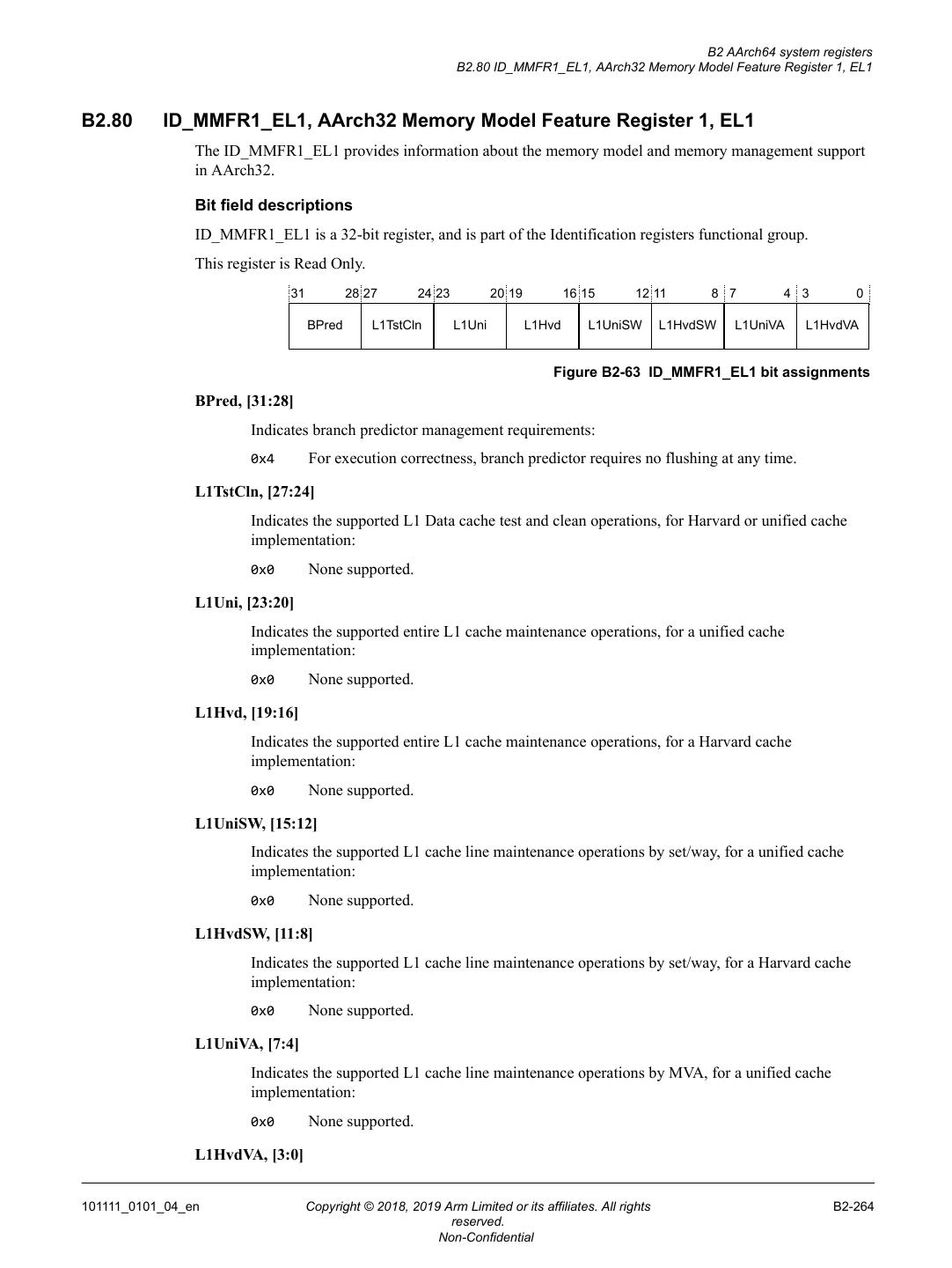


- 快召唤伙伴们来围观吧
- 微博 QQ QQ空间 贴吧
- 文档嵌入链接
- <iframe src="https://www.slidestalk.com/chiptech/arm_cortex_a77_trm_101111_0101_04_en?embed" frame border="0" width="640" height="360" scrolling="no" allowfullscreen="true">复制
- 微信扫一扫分享
Cortex-A 系列处理器Cortex-A77文档分享 |arm_cortex_a77_trm_101111_0101_04_en
分享
点赞
0
收藏
0
下载 0
Cortex-A77相关文档 ARM Cortex-A 系列的Cortex-A77的 ARM 文档集 TARM Cortex-A 系列是一系列用于复杂操作系统和用户应用程序的应用程序处理器。Cortex-A 系列处理器支持 ARM、Thumb 和 Thumb-2 指令集。
Cortex-A77文档集:
Revision: r0-r1 revisions Arm Cortex-A77 MP074 Software Developers Errata Notice Arm Cortex-A77 Core Software Optimization Guide Software Optimization Guide Revision: r1p1 Arm Cortex‑A77 Core Cryptographic Extension Technical Reference Manual Arm Cortex‑A77 Core Technical Reference Manual
包含文档如下: arm_cortex_a77_mp074_software_developer_errata_notice_v9.0 arm_cortex_A77_software_optimization_guide arm_cortex_a77_crypto_trm_101113_0101_02_en arm_cortex_a77_trm_101111_0101_04_en
展开查看详情
1 . Arm® Cortex®-A77 Core Revision: r1p1 Technical Reference Manual Copyright © 2018, 2019 Arm Limited or its affiliates. All rights reserved. 101111_0101_04_en
2 . Arm® Cortex®-A77 Core Arm® Cortex®-A77 Core Technical Reference Manual Copyright © 2018, 2019 Arm Limited or its affiliates. All rights reserved. Release Information Document History Issue Date Confidentiality Change 0000-01 27 April 2018 Confidential First release for r0p0 0100-00 14 September 2018 Confidential First release for r1p0 0101-00 26 May 2019 Non-Confidential First release for r1p1 0101-01 23 August 2019 Non-Confidential Second release for r1p1 0101-02 17 September 2019 Non-Confidential Third release for r1p1 0101-03 25 October 2019 Non-Confidential Fourth release for r1p1 0101-04 31 October 2019 Non-Confidential Fifth release for r1p1 Non-Confidential Proprietary Notice This document is protected by copyright and other related rights and the practice or implementation of the information contained in this document may be protected by one or more patents or pending patent applications. No part of this document may be reproduced in any form by any means without the express prior written permission of Arm. No license, express or implied, by estoppel or otherwise to any intellectual property rights is granted by this document unless specifically stated. Your access to the information in this document is conditional upon your acceptance that you will not use or permit others to use the information for the purposes of determining whether implementations infringe any third party patents. THIS DOCUMENT IS PROVIDED “AS IS”. ARM PROVIDES NO REPRESENTATIONS AND NO WARRANTIES, EXPRESS, IMPLIED OR STATUTORY, INCLUDING, WITHOUT LIMITATION, THE IMPLIED WARRANTIES OF MERCHANTABILITY, SATISFACTORY QUALITY, NON-INFRINGEMENT OR FITNESS FOR A PARTICULAR PURPOSE WITH RESPECT TO THE DOCUMENT. For the avoidance of doubt, Arm makes no representation with respect to, and has undertaken no analysis to identify or understand the scope and content of, third party patents, copyrights, trade secrets, or other rights. This document may include technical inaccuracies or typographical errors. TO THE EXTENT NOT PROHIBITED BY LAW, IN NO EVENT WILL ARM BE LIABLE FOR ANY DAMAGES, INCLUDING WITHOUT LIMITATION ANY DIRECT, INDIRECT, SPECIAL, INCIDENTAL, PUNITIVE, OR CONSEQUENTIAL DAMAGES, HOWEVER CAUSED AND REGARDLESS OF THE THEORY OF LIABILITY, ARISING OUT OF ANY USE OF THIS DOCUMENT, EVEN IF ARM HAS BEEN ADVISED OF THE POSSIBILITY OF SUCH DAMAGES. This document consists solely of commercial items. You shall be responsible for ensuring that any use, duplication or disclosure of this document complies fully with any relevant export laws and regulations to assure that this document or any portion thereof is not exported, directly or indirectly, in violation of such export laws. Use of the word “partner” in reference to Arm’s customers is not intended to create or refer to any partnership relationship with any other company. Arm may make changes to this document at any time and without notice. If any of the provisions contained in these terms conflict with any of the provisions of any click through or signed written agreement covering this document with Arm, then the click through or signed written agreement prevails over and supersedes the conflicting provisions of these terms. This document may be translated into other languages for convenience, and you agree that if there is any conflict between the English version of this document and any translation, the terms of the English version of the Agreement shall prevail. The Arm corporate logo and words marked with ® or ™ are registered trademarks or trademarks of Arm Limited (or its subsidiaries) in the US and/or elsewhere. All rights reserved. Other brands and names mentioned in this document may be the trademarks of their respective owners. Please follow Arm’s trademark usage guidelines at http://www.arm.com/company/policies/ trademarks. 101111_0101_04_en Copyright © 2018, 2019 Arm Limited or its affiliates. All rights 2 reserved. Non-Confidential
3 . Arm® Cortex®-A77 Core Copyright © 2018, 2019 Arm Limited (or its affiliates). All rights reserved. Arm Limited. Company 02557590 registered in England. 110 Fulbourn Road, Cambridge, England CB1 9NJ. LES-PRE-20349 Confidentiality Status This document is Non-Confidential. The right to use, copy and disclose this document may be subject to license restrictions in accordance with the terms of the agreement entered into by Arm and the party that Arm delivered this document to. Unrestricted Access is an Arm internal classification. Product Status The information in this document is Final, that is for a developed product. Web Address www.arm.com 101111_0101_04_en Copyright © 2018, 2019 Arm Limited or its affiliates. All rights 3 reserved. Non-Confidential
4 .
5 .Contents Arm® Cortex®-A77 Core Technical Reference Manual Preface About this book ..................................................... ..................................................... 16 Feedback .................................................................................................................... 21 Part A Functional description Chapter A1 Introduction A1.1 About the core ................................................... ................................................... A1-26 A1.2 Features ................................................................................................................ A1-27 A1.3 Implementation options ............................................ ............................................ A1-28 A1.4 Supported standards and specifications ............................... ............................... A1-29 A1.5 Test features .......................................................................................................... A1-30 A1.6 Design tasks .......................................................................................................... A1-31 A1.7 Product revisions ................................................. ................................................. A1-32 Chapter A2 Technical overview A2.1 Components .......................................................................................................... A2-34 A2.2 Interfaces ....................................................... ....................................................... A2-38 A2.3 About system control .............................................. .............................................. A2-39 A2.4 About the Generic Timer ........................................... ........................................... A2-40 Chapter A3 Clocks, resets, and input synchronization A3.1 About clocks, resets, and input synchronization ......................... ......................... A3-42 A3.2 Asynchronous interface ............................................ ............................................ A3-43 101111_0101_04_en Copyright © 2018, 2019 Arm Limited or its affiliates. All rights 5 reserved. Non-Confidential
6 . Chapter A4 Power management A4.1 About power management .................................................................................... A4-46 A4.2 Voltage domains .................................................................................................... A4-47 A4.3 Power domains .................................................. .................................................. A4-48 A4.4 Architectural clock gating modes ..................................... ..................................... A4-50 A4.5 Power control ........................................................................................................ A4-52 A4.6 Core power modes ................................................................................................ A4-53 A4.7 Encoding for power modes ......................................... ......................................... A4-56 A4.8 Power domain states for power modes ................................ ................................ A4-57 A4.9 Core powerup and powerdown sequences ............................. ............................. A4-58 A4.10 Debug over powerdown ........................................................................................ A4-59 Chapter A5 Memory Management Unit A5.1 About the MMU .................................................. .................................................. A5-62 A5.2 TLB organization ................................................. ................................................. A5-64 A5.3 TLB match process ............................................... ............................................... A5-65 A5.4 Translation table walks .......................................................................................... A5-66 A5.5 MMU memory accesses ........................................................................................ A5-67 A5.6 Specific behaviors on aborts and memory attributes ............................................ A5-68 A5.7 Page-based hardware attributes ..................................... ..................................... A5-70 Chapter A6 Level 1 memory system A6.1 About the L1 memory system ....................................... ....................................... A6-72 A6.2 Cache behavior .................................................. .................................................. A6-73 A6.3 L1 instruction memory system ....................................... ....................................... A6-75 A6.4 L1 data memory system ........................................................................................ A6-77 A6.5 Data prefetching .................................................................................................... A6-79 A6.6 Direct access to internal memory .......................................................................... A6-80 Chapter A7 Level 2 memory system A7.1 About the L2 memory system ....................................... ....................................... A7-98 A7.2 About the L2 cache ............................................... ............................................... A7-99 A7.3 Support for memory types ......................................... ......................................... A7-100 Chapter A8 Reliability, Availability, and Serviceability (RAS) A8.1 Cache ECC and parity ............................................ ............................................ A8-102 A8.2 Cache protection behavior ........................................ ........................................ A8-103 A8.3 Uncorrected errors and data poisoning ............................... ............................... A8-105 A8.4 RAS error types ................................................. ................................................. A8-106 A8.5 Error Synchronization Barrier ...................................... ...................................... A8-107 A8.6 Error recording .................................................................................................... A8-108 A8.7 Error injection ...................................................................................................... A8-109 Chapter A9 Generic Interrupt Controller CPU interface A9.1 About the Generic Interrupt Controller CPU interface .................... .................... A9-112 A9.2 Bypassing the CPU interface ....................................... ....................................... A9-113 Chapter A10 Advanced SIMD and floating-point support A10.1 About the Advanced SIMD and floating-point support ................... ................... A10-116 A10.2 Accessing the feature identification registers .................................................... A10-117 101111_0101_04_en Copyright © 2018, 2019 Arm Limited or its affiliates. All rights 6 reserved. Non-Confidential
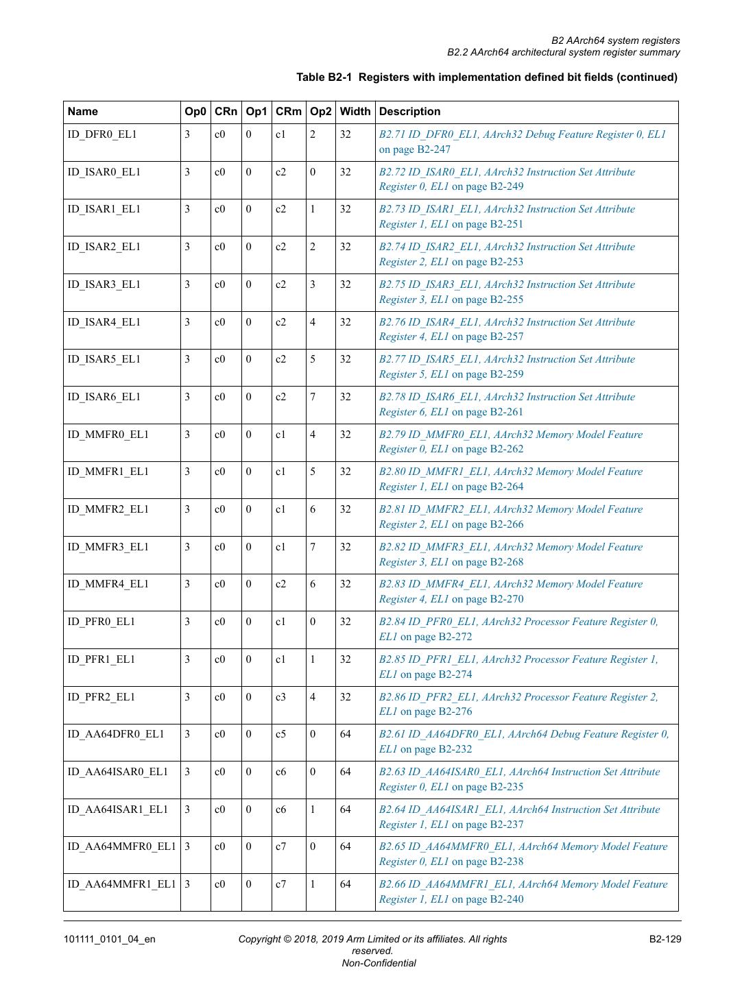
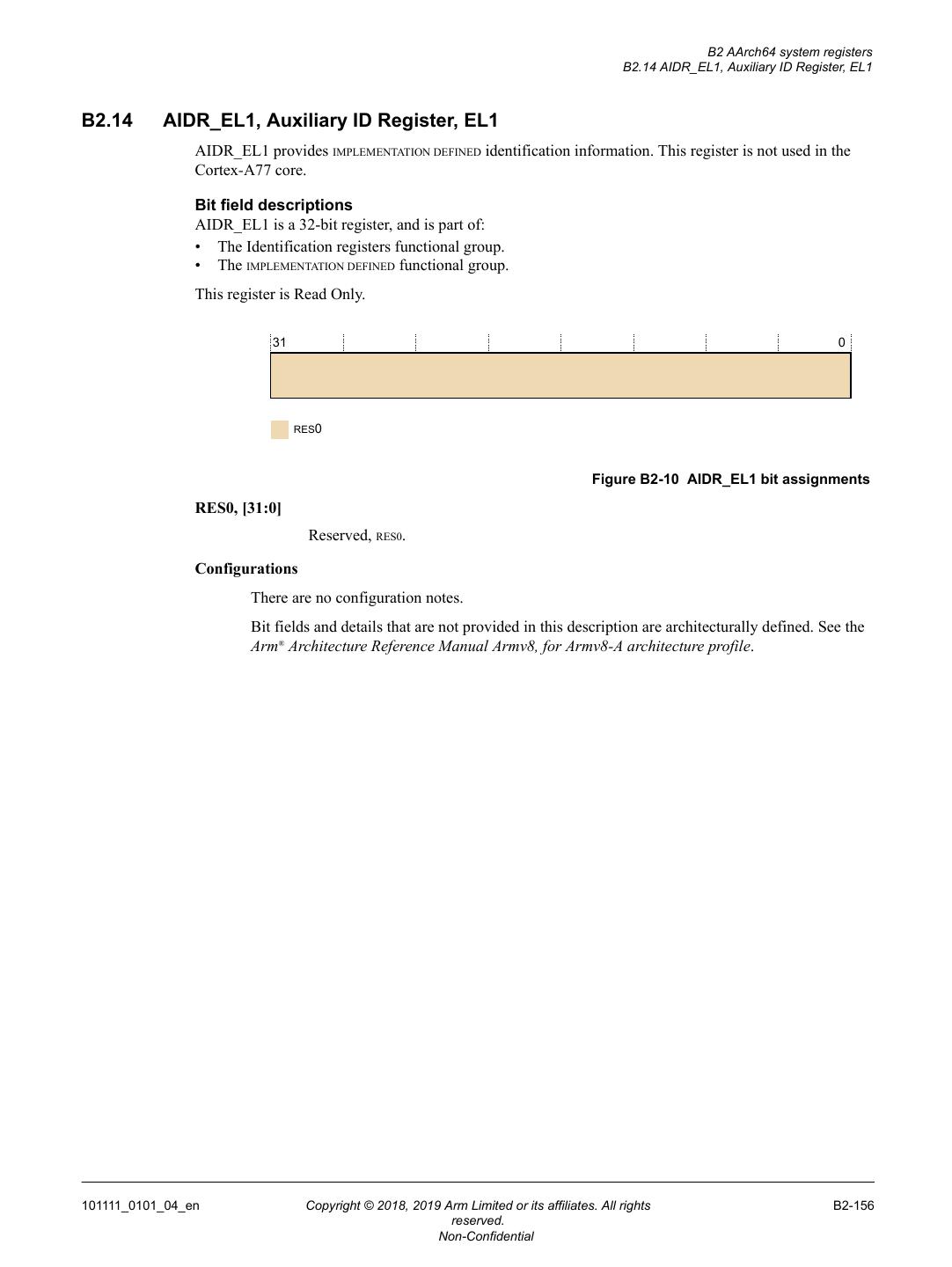
7 .Part B Register descriptions Chapter B1 AArch32 system registers B1.1 AArch32 architectural system register summary ........................ ........................ B1-122 Chapter B2 AArch64 system registers B2.1 AArch64 registers ................................................................................................ B2-126 B2.2 AArch64 architectural system register summary ........................ ........................ B2-127 B2.3 AArch64 implementation defined register summary ..................... ..................... B2-134 B2.4 AArch64 registers by functional group ................................................................ B2-137 B2.5 ACTLR_EL1, Auxiliary Control Register, EL1 .......................... .......................... B2-145 B2.6 ACTLR_EL2, Auxiliary Control Register, EL2 .......................... .......................... B2-146 B2.7 ACTLR_EL3, Auxiliary Control Register, EL3 .......................... .......................... B2-148 B2.8 AFSR0_EL1, Auxiliary Fault Status Register 0, EL1 ..................... ..................... B2-150 B2.9 AFSR0_EL2, Auxiliary Fault Status Register 0, EL2 ..................... ..................... B2-151 B2.10 AFSR0_EL3, Auxiliary Fault Status Register 0, EL3 ..................... ..................... B2-152 B2.11 AFSR1_EL1, Auxiliary Fault Status Register 1, EL1 ..................... ..................... B2-153 B2.12 AFSR1_EL2, Auxiliary Fault Status Register 1, EL2 ..................... ..................... B2-154 B2.13 AFSR1_EL3, Auxiliary Fault Status Register 1, EL3 ..................... ..................... B2-155 B2.14 AIDR_EL1, Auxiliary ID Register, EL1 ................................ ................................ B2-156 B2.15 AMAIR_EL1, Auxiliary Memory Attribute Indirection Register, EL1 .................... B2-157 B2.16 AMAIR_EL2, Auxiliary Memory Attribute Indirection Register, EL2 .................... B2-158 B2.17 AMAIR_EL3, Auxiliary Memory Attribute Indirection Register, EL3 .................... B2-159 B2.18 ATCR_EL1, Auxiliary Translation Control Register, EL1 .................. .................. B2-160 B2.19 ATCR_EL2, Auxiliary Translation Control Register, EL2 .................. .................. B2-162 B2.20 ATCR_EL12 , Alias to Auxiliary Translation Control Register EL1 ...................... B2-164 B2.21 ATCR_EL3, Auxiliary Translation Control Register, EL3 .................. .................. B2-165 B2.22 AVTCR_EL2, Auxiliary Virtualized Translation Control Register, EL2 ........ ........ B2-167 B2.23 CCSIDR_EL1, Cache Size ID Register, EL1 ........................... ........................... B2-169 B2.24 CLIDR_EL1, Cache Level ID Register, EL1 ........................... ........................... B2-171 B2.25 CPACR_EL1, Architectural Feature Access Control Register, EL1 .......... .......... B2-173 B2.26 CPTR_EL2, Architectural Feature Trap Register, EL2 ........................................ B2-174 B2.27 CPTR_EL3, Architectural Feature Trap Register, EL3 ........................................ B2-175 B2.28 CPUACTLR_EL1, CPU Auxiliary Control Register, EL1 .................. .................. B2-176 B2.29 CPUACTLR2_EL1, CPU Auxiliary Control Register 2, EL1 ................................ B2-178 B2.30 CPUACTLR3_EL1, CPU Auxiliary Control Register 3, EL1 ................................ B2-180 B2.31 CPUCFR_EL1, CPU Configuration Register, EL1 .............................................. B2-182 B2.32 CPUECTLR_EL1, CPU Extended Control Register, EL1 ................. ................. B2-184 B2.33 CPUECTLR2_EL1, CPU Extended Control Register2, EL1 .............................. B2-192 B2.34 CPUPCR_EL3, CPU Private Control Register, EL3 ............................................ B2-195 B2.35 CPUPMR_EL3, CPU Private Mask Register, EL3 .............................................. B2-197 B2.36 CPUPOR_EL3, CPU Private Operation Register, EL3 ................... ................... B2-199 B2.37 CPUPSELR_EL3, CPU Private Selection Register, EL3 .................................... B2-201 B2.38 CPUPWRCTLR_EL1, Power Control Register, EL1 ..................... ..................... B2-203 B2.39 CSSELR_EL1, Cache Size Selection Register, EL1 ..................... ..................... B2-206 B2.40 CTR_EL0, Cache Type Register, EL0 ................................ ................................ B2-207 B2.41 DCZID_EL0, Data Cache Zero ID Register, EL0 ................................................ B2-209 B2.42 DISR_EL1, Deferred Interrupt Status Register, EL1 ..................... ..................... B2-210 B2.43 ERRIDR_EL1, Error ID Register, EL1 ................................ ................................ B2-212 B2.44 ERRSELR_EL1, Error Record Select Register, EL1 .......................................... B2-213 101111_0101_04_en Copyright © 2018, 2019 Arm Limited or its affiliates. All rights 7 reserved. Non-Confidential
8 . B2.45 ERXADDR_EL1, Selected Error Record Address Register, EL1 ........................ B2-214 B2.46 ERXCTLR_EL1, Selected Error Record Control Register, EL1 .......................... B2-215 B2.47 ERXFR_EL1, Selected Error Record Feature Register, EL1 .............................. B2-216 B2.48 ERXMISC0_EL1, Selected Error Record Miscellaneous Register 0, EL1 .......... B2-217 B2.49 ERXMISC1_EL1, Selected Error Record Miscellaneous Register 1, EL1 .......... B2-218 B2.50 ERXPFGCDN_EL1, Selected Error Pseudo Fault Generation Count Down Register, EL1 ...................................................................................................................... B2-219 B2.51 ERXPFGCTL_EL1, Selected Error Pseudo Fault Generation Control Register, EL1 .... ............................................................................................................................. B2-220 B2.52 ERXPFGF_EL1, Selected Pseudo Fault Generation Feature Register, EL1 ...... B2-222 B2.53 ERXSTATUS_EL1, Selected Error Record Primary Status Register, EL1 .......... B2-223 B2.54 ESR_EL1, Exception Syndrome Register, EL1 ......................... ......................... B2-224 B2.55 ESR_EL2, Exception Syndrome Register, EL2 ......................... ......................... B2-225 B2.56 ESR_EL3, Exception Syndrome Register, EL3 ......................... ......................... B2-226 B2.57 HACR_EL2, Hyp Auxiliary Configuration Register, EL2 ...................................... B2-227 B2.58 HCR_EL2, Hypervisor Configuration Register, EL2 ............................................ B2-228 B2.59 ID_AA64AFR0_EL1, AArch64 Auxiliary Feature Register 0 ............... ............... B2-230 B2.60 ID_AA64AFR1_EL1, AArch64 Auxiliary Feature Register 1 ............... ............... B2-231 B2.61 ID_AA64DFR0_EL1, AArch64 Debug Feature Register 0, EL1 ............ ............ B2-232 B2.62 ID_AA64DFR1_EL1, AArch64 Debug Feature Register 1, EL1 ............ ............ B2-234 B2.63 ID_AA64ISAR0_EL1, AArch64 Instruction Set Attribute Register 0, EL1 ..... ..... B2-235 B2.64 ID_AA64ISAR1_EL1, AArch64 Instruction Set Attribute Register 1, EL1 ..... ..... B2-237 B2.65 ID_AA64MMFR0_EL1, AArch64 Memory Model Feature Register 0, EL1 .... .... B2-238 B2.66 ID_AA64MMFR1_EL1, AArch64 Memory Model Feature Register 1, EL1 .... .... B2-240 B2.67 ID_AA64MMFR2_EL1, AArch64 Memory Model Feature Register 2, EL1 .... .... B2-242 B2.68 ID_AA64PFR0_EL1, AArch64 Processor Feature Register 0, EL1 .................... B2-243 B2.69 ID_AA64PFR1_EL1, AArch64 Processor Feature Register 1, EL1 .................... B2-245 B2.70 ID_AFR0_EL1, AArch32 Auxiliary Feature Register 0, EL1 ............... ............... B2-246 B2.71 ID_DFR0_EL1, AArch32 Debug Feature Register 0, EL1 .................................. B2-247 B2.72 ID_ISAR0_EL1, AArch32 Instruction Set Attribute Register 0, EL1 .................... B2-249 B2.73 ID_ISAR1_EL1, AArch32 Instruction Set Attribute Register 1, EL1 .................... B2-251 B2.74 ID_ISAR2_EL1, AArch32 Instruction Set Attribute Register 2, EL1 .................... B2-253 B2.75 ID_ISAR3_EL1, AArch32 Instruction Set Attribute Register 3, EL1 .................... B2-255 B2.76 ID_ISAR4_EL1, AArch32 Instruction Set Attribute Register 4, EL1 .................... B2-257 B2.77 ID_ISAR5_EL1, AArch32 Instruction Set Attribute Register 5, EL1 .................... B2-259 B2.78 ID_ISAR6_EL1, AArch32 Instruction Set Attribute Register 6, EL1 .................... B2-261 B2.79 ID_MMFR0_EL1, AArch32 Memory Model Feature Register 0, EL1 .................. B2-262 B2.80 ID_MMFR1_EL1, AArch32 Memory Model Feature Register 1, EL1 .................. B2-264 B2.81 ID_MMFR2_EL1, AArch32 Memory Model Feature Register 2, EL1 .................. B2-266 B2.82 ID_MMFR3_EL1, AArch32 Memory Model Feature Register 3, EL1 .................. B2-268 B2.83 ID_MMFR4_EL1, AArch32 Memory Model Feature Register 4, EL1 .................. B2-270 B2.84 ID_PFR0_EL1, AArch32 Processor Feature Register 0, EL1 .............. .............. B2-272 B2.85 ID_PFR1_EL1, AArch32 Processor Feature Register 1, EL1 .............. .............. B2-274 B2.86 ID_PFR2_EL1, AArch32 Processor Feature Register 2, EL1 .............. .............. B2-276 B2.87 LORC_EL1, LORegion Control Register, EL1 .......................... .......................... B2-277 B2.88 LORID_EL1, LORegion ID Register, EL1 ............................. ............................. B2-278 B2.89 LORN_EL1, LORegion Number Register, EL1 ......................... ......................... B2-279 B2.90 MDCR_EL3, Monitor Debug Configuration Register, EL3 ................. ................. B2-280 B2.91 MIDR_EL1, Main ID Register, EL1 ...................................................................... B2-282 B2.92 MPIDR_EL1, Multiprocessor Affinity Register, EL1 ...................... ...................... B2-283 101111_0101_04_en Copyright © 2018, 2019 Arm Limited or its affiliates. All rights 8 reserved. Non-Confidential
9 . B2.93 PAR_EL1, Physical Address Register, EL1 ............................ ............................ B2-285 B2.94 REVIDR_EL1, Revision ID Register, EL1 ............................. ............................. B2-286 B2.95 RMR_EL3, Reset Management Register ............................................................ B2-287 B2.96 RVBAR_EL3, Reset Vector Base Address Register, EL3 ................. ................. B2-288 B2.97 SCTLR_EL1, System Control Register, EL1 ........................... ........................... B2-289 B2.98 SCTLR_EL2, System Control Register, EL2 ........................... ........................... B2-291 B2.99 SCTLR_EL3, System Control Register, EL3 ........................... ........................... B2-292 B2.100 TCR_EL1, Translation Control Register, EL1 ...................................................... B2-294 B2.101 TCR_EL2, Translation Control Register, EL2 ...................................................... B2-295 B2.102 TCR_EL3, Translation Control Register, EL3 ...................................................... B2-296 B2.103 TTBR0_EL1, Translation Table Base Register 0, EL1 ........................................ B2-297 B2.104 TTBR0_EL2, Translation Table Base Register 0, EL2 ........................................ B2-298 B2.105 TTBR0_EL3, Translation Table Base Register 0, EL3 ................... ................... B2-299 B2.106 TTBR1_EL1, Translation Table Base Register 1, EL1 ........................................ B2-300 B2.107 TTBR1_EL2, Translation Table Base Register 1, EL2 ........................................ B2-301 B2.108 VDISR_EL2, Virtual Deferred Interrupt Status Register, EL2 .............. .............. B2-302 B2.109 VSESR_EL2, Virtual SError Exception Syndrome Register ............... ............... B2-303 B2.110 VTCR_EL2, Virtualization Translation Control Register, EL2 .............................. B2-304 B2.111 VTTBR_EL2, Virtualization Translation Table Base Register, EL2 .......... .......... B2-305 Chapter B3 Error system registers B3.1 Error system register summary ..................................... ..................................... B3-308 B3.2 ERR0ADDR, Error Record Address Register .......................... .......................... B3-309 B3.3 ERR0CTLR, Error Record Control Register ........................................................ B3-310 B3.4 ERR0FR, Error Record Feature Register ............................. ............................. B3-312 B3.5 ERR0MISC0, Error Record Miscellaneous Register 0 ........................................ B3-314 B3.6 ERR0MISC1, Error Record Miscellaneous Register 1 ........................................ B3-317 B3.7 ERR0PFGCDN, Error Pseudo Fault Generation Count Down Register ...... ...... B3-318 B3.8 ERR0PFGCTL, Error Pseudo Fault Generation Control Register ........... ........... B3-319 B3.9 ERR0PFGF, Error Pseudo Fault Generation Feature Register ............. ............. B3-321 B3.10 ERR0STATUS, Error Record Primary Status Register ................... ................... B3-323 Chapter B4 GIC registers B4.1 CPU interface registers ........................................... ........................................... B4-329 B4.2 AArch64 physical GIC CPU interface system register summary ............ ............ B4-330 B4.3 ICC_AP0R0_EL1, Interrupt Controller Active Priorities Group 0 Register 0, EL1 .... ............................................................................................................................. B4-331 B4.4 ICC_AP1R0_EL1, Interrupt Controller Active Priorities Group 1 Register 0 EL1 B4-332 B4.5 ICC_BPR0_EL1, Interrupt Controller Binary Point Register 0, EL1 .................... B4-333 B4.6 ICC_BPR1_EL1, Interrupt Controller Binary Point Register 1, EL1 .................... B4-334 B4.7 ICC_CTLR_EL1, Interrupt Controller Control Register, EL1 ............... ............... B4-335 B4.8 ICC_CTLR_EL3, Interrupt Controller Control Register, EL3 ............... ............... B4-337 B4.9 ICC_SRE_EL1, Interrupt Controller System Register Enable Register, EL1 ...... B4-339 B4.10 ICC_SRE_EL2, Interrupt Controller System Register Enable register, EL2 ... ... B4-340 B4.11 ICC_SRE_EL3, Interrupt Controller System Register Enable register, EL3 ... ... B4-342 B4.12 AArch64 virtual GIC CPU interface register summary ........................................ B4-344 B4.13 ICV_AP0R0_EL1, Interrupt Controller Virtual Active Priorities Group 0 Register 0, EL1 ...................................................................................................................... B4-345 B4.14 ICV_AP1R0_EL1, Interrupt Controller Virtual Active Priorities Group 1 Register 0, EL1 ...................................................................................................................... B4-346 101111_0101_04_en Copyright © 2018, 2019 Arm Limited or its affiliates. All rights 9 reserved. Non-Confidential
10 . B4.15 ICV_BPR0_EL1, Interrupt Controller Virtual Binary Point Register 0, EL1 .... .... B4-347 B4.16 ICV_BPR1_EL1, Interrupt Controller Virtual Binary Point Register 1, EL1 .... .... B4-348 B4.17 ICV_CTLR_EL1, Interrupt Controller Virtual Control Register, EL1 .................... B4-349 B4.18 AArch64 virtual interface control system register summary ................................ B4-351 B4.19 ICH_AP0R0_EL2, Interrupt Controller Hyp Active Priorities Group 0 Register 0, EL2 .... ............................................................................................................................. B4-352 B4.20 ICH_AP1R0_EL2, Interrupt Controller Hyp Active Priorities Group 1 Register 0, EL2 .... ............................................................................................................................. B4-353 B4.21 ICH_HCR_EL2, Interrupt Controller Hyp Control Register, EL2 ............ ............ B4-354 B4.22 ICH_VMCR_EL2, Interrupt Controller Virtual Machine Control Register, EL2 .... B4-357 B4.23 ICH_VTR_EL2, Interrupt Controller VGIC Type Register, EL2 ............. ............. B4-359 Chapter B5 Advanced SIMD and floating-point registers B5.1 AArch64 register summary .................................................................................. B5-362 B5.2 FPCR, Floating-point Control Register ................................................................ B5-363 B5.3 FPSR, Floating-point Status Register ................................ ................................ B5-365 B5.4 MVFR0_EL1, Media and VFP Feature Register 0, EL1 ...................................... B5-367 B5.5 MVFR1_EL1, Media and VFP Feature Register 1, EL1 ...................................... B5-369 B5.6 MVFR2_EL1, Media and VFP Feature Register 2, EL1 ...................................... B5-371 B5.7 AArch32 register summary .................................................................................. B5-373 B5.8 FPSCR, Floating-Point Status and Control Register ..................... ..................... B5-374 Part C Debug descriptions Chapter C1 Debug C1.1 About debug methods ............................................ ............................................ C1-382 C1.2 Debug register interfaces .................................................................................... C1-383 C1.3 Debug events ...................................................................................................... C1-385 C1.4 External debug interface .......................................... .......................................... C1-386 Chapter C2 Performance Monitor Unit C2.1 About the PMU .................................................................................................... C2-388 C2.2 PMU functional description ........................................ ........................................ C2-389 C2.3 PMU events .................................................... .................................................... C2-390 C2.4 PMU interrupts .................................................................................................... C2-399 C2.5 Exporting PMU events ........................................................................................ C2-400 Chapter C3 Activity Monitor Unit C3.1 About the AMU .................................................................................................... C3-402 C3.2 Accessing the activity monitors ..................................... ..................................... C3-403 C3.3 AMU counters .................................................. .................................................. C3-404 C3.4 AMU events .................................................... .................................................... C3-405 Chapter C4 Embedded Trace Macrocell C4.1 About the ETM .................................................................................................... C4-408 C4.2 ETM trace unit generation options and resources .............................................. C4-409 C4.3 ETM trace unit functional description .................................................................. C4-411 C4.4 Resetting the ETM .............................................................................................. C4-412 C4.5 Programming and reading ETM trace unit registers ..................... ..................... C4-413 C4.6 ETM trace unit register interfaces ................................... ................................... C4-414 101111_0101_04_en Copyright © 2018, 2019 Arm Limited or its affiliates. All rights 10 reserved. Non-Confidential
11 . C4.7 Interaction with the PMU and Debug .................................................................. C4-415 Part D Debug registers Chapter D1 AArch32 debug registers D1.1 AArch32 debug register summary ................................... ................................... D1-420 Chapter D2 AArch64 debug registers D2.1 AArch64 debug register summary ................................... ................................... D2-422 D2.2 DBGBCRn_EL1, Debug Breakpoint Control Registers, EL1 .............................. D2-424 D2.3 DBGCLAIMSET_EL1, Debug Claim Tag Set Register, EL1 ............... ............... D2-427 D2.4 DBGWCRn_EL1, Debug Watchpoint Control Registers, EL1 .............. .............. D2-428 Chapter D3 Memory-mapped debug registers D3.1 Memory-mapped debug register summary ............................ ............................ D3-432 D3.2 EDCIDR0, External Debug Component Identification Register 0 ........... ........... D3-436 D3.3 EDCIDR1, External Debug Component Identification Register 1 ........... ........... D3-437 D3.4 EDCIDR2, External Debug Component Identification Register 2 ........... ........... D3-438 D3.5 EDCIDR3, External Debug Component Identification Register 3 ........... ........... D3-439 D3.6 EDDEVID, External Debug Device ID Register 0 ....................... ....................... D3-440 D3.7 EDDEVID1, External Debug Device ID Register 1 ...................... ...................... D3-441 D3.8 EDPIDR0, External Debug Peripheral Identification Register 0 .......................... D3-442 D3.9 EDPIDR1, External Debug Peripheral Identification Register 1 .......................... D3-443 D3.10 EDPIDR2, External Debug Peripheral Identification Register 2 .......................... D3-444 D3.11 EDPIDR3, External Debug Peripheral Identification Register 3 .......................... D3-445 D3.12 EDPIDR4, External Debug Peripheral Identification Register 4 .......................... D3-446 D3.13 EDPIDRn, External Debug Peripheral Identification Registers 5-7 .......... .......... D3-447 D3.14 EDRCR, External Debug Reserve Control Register ..................... ..................... D3-448 Chapter D4 AArch32 PMU registers D4.1 AArch32 PMU register summary .................................... .................................... D4-450 D4.2 PMCEID0, Performance Monitors Common Event Identification Register 0 ...... D4-452 D4.3 PMCEID1, Performance Monitors Common Event Identification Register 1 ...... D4-455 D4.4 PMCR, Performance Monitors Control Register ........................ ........................ D4-457 Chapter D5 AArch64 PMU registers D5.1 AArch64 PMU register summary .................................... .................................... D5-462 D5.2 PMCEID0_EL0, Performance Monitors Common Event Identification Register 0, EL0 .. ............................................................................................................................. D5-464 D5.3 PMCEID1_EL0, Performance Monitors Common Event Identification Register 1, EL0 .. ............................................................................................................................. D5-467 D5.4 PMCR_EL0, Performance Monitors Control Register, EL0 ................ ................ D5-469 Chapter D6 Memory-mapped PMU registers D6.1 Memory-mapped PMU register summary ............................. ............................. D6-472 D6.2 PMCFGR, Performance Monitors Configuration Register .................................. D6-476 D6.3 PMCIDR0, Performance Monitors Component Identification Register 0 ............ D6-477 D6.4 PMCIDR1, Performance Monitors Component Identification Register 1 ............ D6-478 D6.5 PMCIDR2, Performance Monitors Component Identification Register 2 ............ D6-479 D6.6 PMCIDR3, Performance Monitors Component Identification Register 3 ............ D6-480 D6.7 PMPIDR0, Performance Monitors Peripheral Identification Register 0 ....... ....... D6-481 101111_0101_04_en Copyright © 2018, 2019 Arm Limited or its affiliates. All rights 11 reserved. Non-Confidential
12 . D6.8 PMPIDR1, Performance Monitors Peripheral Identification Register 1 ....... ....... D6-482 D6.9 PMPIDR2, Performance Monitors Peripheral Identification Register 2 ....... ....... D6-483 D6.10 PMPIDR3, Performance Monitors Peripheral Identification Register 3 ....... ....... D6-484 D6.11 PMPIDR4, Performance Monitors Peripheral Identification Register 4 ....... ....... D6-485 D6.12 PMPIDRn, Performance Monitors Peripheral Identification Register 5-7 ..... ..... D6-486 Chapter D7 PMU snapshot registers D7.1 PMU snapshot register summary ........................................................................ D7-488 D7.2 PMPCSSR, PMU Snapshot Program Counter Sample Register ........................ D7-489 D7.3 PMCIDSSR, PMU Snapshot CONTEXTIDR_EL1 Sample Register ......... ......... D7-490 D7.4 PMCID2SSR, PMU Snapshot CONTEXTIDR_EL2 Sample Register ........ ........ D7-491 D7.5 PMSSSR, PMU Snapshot Status Register ............................ ............................ D7-492 D7.6 PMOVSSR, PMU Snapshot Overflow Status Register ................... ................... D7-493 D7.7 PMCCNTSR, PMU Snapshot Cycle Counter Register ................... ................... D7-494 D7.8 PMEVCNTSRn, PMU Snapshot Cycle Counter Registers 0-5 ............. ............. D7-495 D7.9 PMSSCR, PMU Snapshot Capture Register ...................................................... D7-496 Chapter D8 AArch64 AMU registers D8.1 AArch64 AMU register summary .................................... .................................... D8-498 D8.2 AMCNTENCLR_EL0, Activity Monitors Count Enable Clear Register, EL0 ... ... D8-499 D8.3 AMCNTENSET_EL0, Activity Monitors Count Enable Set Register, EL0 ..... ..... D8-500 D8.4 AMCFGR_EL0, Activity Monitors Configuration Register, EL0 ............. ............. D8-501 D8.5 AMUSERENR_EL0, Activity Monitor EL0 Enable access, EL0 .......................... D8-503 D8.6 AMEVCNTRn_EL0, Activity Monitor Event Counter Register, EL0 .......... .......... D8-505 D8.7 AMEVTYPERn_EL0, Activity Monitor Event Type Register, EL0 ........... ........... D8-506 Chapter D9 Memory-mapped AMU registers D9.1 Memory-mapped AMU register summary ............................. ............................. D9-510 Chapter D10 ETM registers D10.1 ETM register summary ...................................................................................... D10-513 D10.2 TRCACATRn, Address Comparator Access Type Registers 0-7 ...................... D10-517 D10.3 TRCACVRn, Address Comparator Value Registers 0-7 ................. ................. D10-519 D10.4 TRCAUTHSTATUS, Authentication Status Register .................... .................... D10-520 D10.5 TRCAUXCTLR, Auxiliary Control Register ........................... ........................... D10-521 D10.6 TRCBBCTLR, Branch Broadcast Control Register ..................... ..................... D10-523 D10.7 TRCCCCTLR, Cycle Count Control Register ......................... ......................... D10-524 D10.8 TRCCIDCCTLR0, Context ID Comparator Control Register 0 ............ ............ D10-525 D10.9 TRCCIDCVR0, Context ID Comparator Value Register 0 ................ ................ D10-526 D10.10 TRCCIDR0, ETM Component Identification Register 0 .................................... D10-527 D10.11 TRCCIDR1, ETM Component Identification Register 1 .................................... D10-528 D10.12 TRCCIDR2, ETM Component Identification Register 2 .................................... D10-529 D10.13 TRCCIDR3, ETM Component Identification Register 3 .................................... D10-530 D10.14 TRCCLAIMCLR, Claim Tag Clear Register ........................... ........................... D10-531 D10.15 TRCCLAIMSET, Claim Tag Set Register .......................................................... D10-532 D10.16 TRCCNTCTLR0, Counter Control Register 0 ......................... ......................... D10-533 D10.17 TRCCNTCTLR1, Counter Control Register 1 ......................... ......................... D10-535 D10.18 TRCCNTRLDVRn, Counter Reload Value Registers 0-1 ................ ................ D10-537 D10.19 TRCCNTVRn, Counter Value Registers 0-1 .......................... .......................... D10-538 D10.20 TRCCONFIGR, Trace Configuration Register ......................... ......................... D10-539 D10.21 TRCDEVAFF0, Device Affinity Register 0 ............................ ............................ D10-542 101111_0101_04_en Copyright © 2018, 2019 Arm Limited or its affiliates. All rights 12 reserved. Non-Confidential
13 . D10.22 TRCDEVAFF1, Device Affinity Register 1 ............................ ............................ D10-543 D10.23 TRCDEVARCH, Device Architecture Register .................................................. D10-544 D10.24 TRCDEVID, Device ID Register ........................................................................ D10-545 D10.25 TRCDEVTYPE, Device Type Register .............................................................. D10-546 D10.26 TRCEVENTCTL0R, Event Control 0 Register .................................................. D10-547 D10.27 TRCEVENTCTL1R, Event Control 1 Register .................................................. D10-549 D10.28 TRCEXTINSELR, External Input Select Register ...................... ...................... D10-550 D10.29 TRCIDR0, ID Register 0 ......................................... ......................................... D10-551 D10.30 TRCIDR1, ID Register 1 ......................................... ......................................... D10-553 D10.31 TRCIDR2, ID Register 2 ......................................... ......................................... D10-554 D10.32 TRCIDR3, ID Register 3 ......................................... ......................................... D10-556 D10.33 TRCIDR4, ID Register 4 ......................................... ......................................... D10-558 D10.34 TRCIDR5, ID Register 5 ......................................... ......................................... D10-560 D10.35 TRCIDR8, ID Register 8 ......................................... ......................................... D10-562 D10.36 TRCIDR9, ID Register 9 ......................................... ......................................... D10-563 D10.37 TRCIDR10, ID Register 10 ....................................... ....................................... D10-564 D10.38 TRCIDR11, ID Register 11 ................................................................................ D10-565 D10.39 TRCIDR12, ID Register 12 ....................................... ....................................... D10-566 D10.40 TRCIDR13, ID Register 13 ....................................... ....................................... D10-567 D10.41 TRCIMSPEC0, IMPLEMENTATION SPECIFIC Register 0 ............... ............... D10-568 D10.42 TRCITATBCTR0, Trace Integration Test ATB Control Register 0 .......... .......... D10-569 D10.43 TRCITATBCTR1, Trace Integration Test ATB Control Register 1 .......... .......... D10-570 D10.44 TRCITATBCTR2, Trace Integration Test ATB Control Register 2 .......... .......... D10-571 D10.45 TRCITATBDATA0, Trace Integration Test ATB Data Register 0 ........................ D10-572 D10.46 TRCITCTRL, Trace Integration Mode Control register .................. .................. D10-573 D10.47 TRCITMISCIN, Trace Integration Miscellaneous Input Register ........... ........... D10-574 D10.48 TRCITMISCOUT, Trace Integration Miscellaneous Outputs Register ....... ....... D10-575 D10.49 TRCLAR, Software Lock Access Register ........................................................ D10-576 D10.50 TRCLSR, Software Lock Status Register ............................ ............................ D10-577 D10.51 TRCCNTVRn, Counter Value Registers 0-1 .......................... .......................... D10-578 D10.52 TRCOSLAR, OS Lock Access Register ............................................................ D10-579 D10.53 TRCOSLSR, OS Lock Status Register .............................. .............................. D10-580 D10.54 TRCPDCR, Power Down Control Register ........................... ........................... D10-581 D10.55 TRCPDSR, Power Down Status Register ............................ ............................ D10-582 D10.56 TRCPIDR0, ETM Peripheral Identification Register 0 ................... ................... D10-583 D10.57 TRCPIDR1, ETM Peripheral Identification Register 1 ................... ................... D10-584 D10.58 TRCPIDR2, ETM Peripheral Identification Register 2 ................... ................... D10-585 D10.59 TRCPIDR3, ETM Peripheral Identification Register 3 ................... ................... D10-586 D10.60 TRCPIDR4, ETM Peripheral Identification Register 4 ................... ................... D10-587 D10.61 TRCPIDRn, ETM Peripheral Identification Registers 5-7 ................ ................ D10-588 D10.62 TRCPRGCTLR, Programming Control Register ....................... ....................... D10-589 D10.63 TRCRSCTLRn, Resource Selection Control Registers 2-16 ............................ D10-590 D10.64 TRCSEQEVRn, Sequencer State Transition Control Registers 0-2 ........ ........ D10-591 D10.65 TRCSEQRSTEVR, Sequencer Reset Control Register .................................... D10-593 D10.66 TRCSEQSTR, Sequencer State Register ............................ ............................ D10-594 D10.67 TRCSSCCR0, Single-Shot Comparator Control Register 0 .............. .............. D10-595 D10.68 TRCSSCSR0, Single-Shot Comparator Status Register 0 ............... ............... D10-596 D10.69 TRCSTATR, Status Register ...................................... ...................................... D10-597 D10.70 TRCSYNCPR, Synchronization Period Register .............................................. D10-598 D10.71 TRCTRACEIDR, Trace ID Register ................................. ................................. D10-599 101111_0101_04_en Copyright © 2018, 2019 Arm Limited or its affiliates. All rights 13 reserved. Non-Confidential
14 . D10.72 TRCTSCTLR, Global Timestamp Control Register ..................... ..................... D10-600 D10.73 TRCVICTLR, ViewInst Main Control Register ......................... ......................... D10-601 D10.74 TRCVIIECTLR, ViewInst Include-Exclude Control Register .............. .............. D10-603 D10.75 TRCVISSCTLR, ViewInst Start-Stop Control Register .................. .................. D10-604 D10.76 TRCVMIDCVR0, VMID Comparator Value Register 0 ...................................... D10-605 D10.77 TRCVMIDCCTLR0, Virtual context identifier Comparator Control Register 0 D10-606 Part E Appendices Appendix A Cortex®-A77 Core AArch32 UNPREDICTABLE behaviors A.1 Use of R15 by Instruction ...................................... ...................................... Appx-A-610 A.2 Load/Store accesses crossing page boundaries .................... .................... Appx-A-611 A.3 Armv8 Debug UNPREDICTABLE behaviors ....................... ....................... Appx-A-612 A.4 Other UNPREDICTABLE behaviors ............................................................ Appx-A-615 Appendix B Revisions B.1 Revisions .................................................. .................................................. Appx-B-618 101111_0101_04_en Copyright © 2018, 2019 Arm Limited or its affiliates. All rights 14 reserved. Non-Confidential
15 .Preface This preface introduces the Arm® Cortex®‑A77 Core Technical Reference Manual. It contains the following: • About this book on page 16. • Feedback on page 21. 101111_0101_04_en Copyright © 2018, 2019 Arm Limited or its affiliates. All rights 15 reserved. Non-Confidential
16 . Preface Product revision status About this book This Technical Reference Manual is for the Cortex®‑A77 core. It provides reference documentation and contains programming details for registers. It also describes the memory system, the caches, the interrupts, and the debug features. Product revision status The rmpn identifier indicates the revision status of the product described in this book, for example, r1p2, where: rm Identifies the major revision of the product, for example, r1. pn Identifies the minor revision or modification status of the product, for example, p2. Intended audience This manual is for system designers, system integrators, and programmers who are designing or programming a System-on-Chip (SoC) that uses an Arm core. Using this book This book is organized into the following chapters: Part A Functional description This part describes the main functionality of the Cortex‑A77 core. Chapter A1 Introduction This chapter provides an overview of the Cortex‑A77 core and its features. Chapter A2 Technical overview This chapter describes the structure of the Cortex‑A77 core. Chapter A3 Clocks, resets, and input synchronization This chapter describes the clocks, resets, and input synchronization of the Cortex‑A77 core. Chapter A4 Power management This chapter describes the power domains and the power modes in the Cortex‑A77 core. Chapter A5 Memory Management Unit This chapter describes the Cortex‑A77 core Memory Management Unit (MMU). Chapter A6 Level 1 memory system This chapter describes the L1 instruction cache and data cache that make up the L1 memory system. Chapter A7 Level 2 memory system This chapter describes the L2 memory system. Chapter A8 Reliability, Availability, and Serviceability (RAS) This chapter describes the RAS features implemented in the Cortex‑A77 core. Chapter A9 Generic Interrupt Controller CPU interface This chapter describes the Cortex‑A77 core implementation of the Arm Generic Interrupt Controller (GIC) CPU interface. Chapter A10 Advanced SIMD and floating-point support This chapter describes the Advanced SIMD and floating-point features and registers in the Cortex‑A77 core. The unit in charge of handling the Advanced SIMD and floating-point features is also referred to as the data engine in this manual. Part B Register descriptions This part describes the non-debug registers of the Cortex‑A77 core. 101111_0101_04_en Copyright © 2018, 2019 Arm Limited or its affiliates. All rights 16 reserved. Non-Confidential
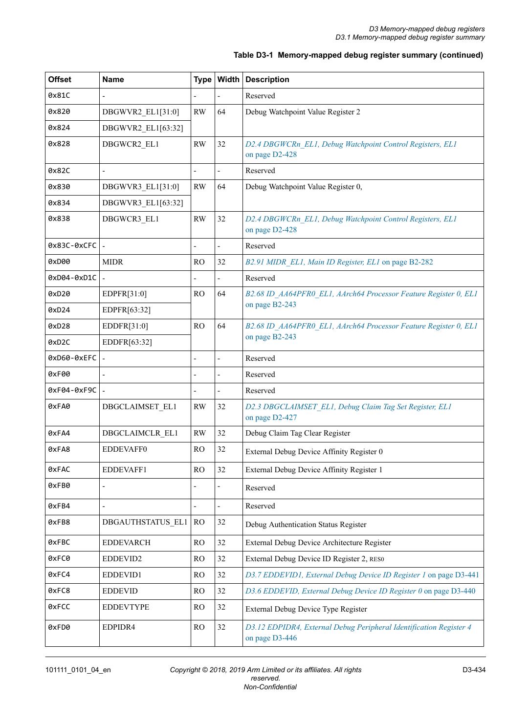
17 . Preface Using this book Chapter B1 AArch32 system registers This chapter describes the system registers in the AArch32 state. Chapter B2 AArch64 system registers This chapter describes the system registers in the AArch64 state. Chapter B3 Error system registers This chapter describes the error registers accessed by the AArch64 error registers. Chapter B4 GIC registers This chapter describes the GIC registers. Chapter B5 Advanced SIMD and floating-point registers This chapter describes the Advanced SIMD and floating-point registers. Part C Debug descriptions This part describes the debug functionality of the Cortex‑A77 core. Chapter C1 Debug This chapter describes the Cortex‑A77 core debug registers and shows examples of how to use them. Chapter C2 Performance Monitor Unit This chapter describes the Performance Monitor Unit (PMU) and the registers that it uses. Chapter C3 Activity Monitor Unit This chapter describes the Activity Monitor Unit (AMU). Chapter C4 Embedded Trace Macrocell This chapter describes the ETM for the Cortex‑A77 core. Part D Debug registers This part describes the debug registers of the Cortex‑A77 core. Chapter D1 AArch32 debug registers This chapter describes the debug registers in the AArch32 Execution state and shows examples of how to use them. Chapter D2 AArch64 debug registers This chapter describes the debug registers in the AArch64 Execution state and shows examples of how to use them. Chapter D3 Memory-mapped debug registers This chapter describes the memory-mapped debug registers and shows examples of how to use them. Chapter D4 AArch32 PMU registers This chapter describes the AArch32 PMU registers and shows examples of how to use them. Chapter D5 AArch64 PMU registers This chapter describes the AArch64 PMU registers and shows examples of how to use them. Chapter D6 Memory-mapped PMU registers This chapter describes the memory-mapped PMU registers and shows examples of how to use them. Chapter D7 PMU snapshot registers PMU snapshot registers are an IMPLEMENTATION DEFINED extension to an Armv8‑A compliant PMU to support an external core monitor that connects to a system profiler. Chapter D8 AArch64 AMU registers This chapter describes the AArch64 AMU registers and shows examples of how to use them. Chapter D9 Memory-mapped AMU registers This chapter describes the memory-mapped AMU registers. The memory-mapped interface provides read-only access to the AMU registers via the external debug interface. 101111_0101_04_en Copyright © 2018, 2019 Arm Limited or its affiliates. All rights 17 reserved. Non-Confidential
18 . Preface Using this book Chapter D10 ETM registers This chapter describes the ETM registers. Part E Appendices This part describes the appendices of the Cortex‑A77 core. Appendix A Cortex®-A77 Core AArch32 UNPREDICTABLE behaviors This appendix describes the cases in which the Cortex‑A77 core implementation diverges from the preferred behavior described in Armv8 AArch32 UNPREDICTABLE behaviors. Appendix B Revisions This appendix describes the technical changes between released issues of this book. Glossary The Arm® Glossary is a list of terms used in Arm documentation, together with definitions for those terms. The Arm Glossary does not contain terms that are industry standard unless the Arm meaning differs from the generally accepted meaning. See the Arm® Glossary for more information. Typographic conventions italic Introduces special terminology, denotes cross-references, and citations. bold Highlights interface elements, such as menu names. Denotes signal names. Also used for terms in descriptive lists, where appropriate. monospace Denotes text that you can enter at the keyboard, such as commands, file and program names, and source code. monospace Denotes a permitted abbreviation for a command or option. You can enter the underlined text instead of the full command or option name. monospace italic Denotes arguments to monospace text where the argument is to be replaced by a specific value. monospace bold Denotes language keywords when used outside example code. <and> Encloses replaceable terms for assembler syntax where they appear in code or code fragments. For example: MRC p15, 0, <Rd>, <CRn>, <CRm>, <Opcode_2> SMALL CAPITALS Used in body text for a few terms that have specific technical meanings, that are defined in the Arm® Glossary. For example, IMPLEMENTATION DEFINED, IMPLEMENTATION SPECIFIC, UNKNOWN, and UNPREDICTABLE. Timing diagrams The following figure explains the components used in timing diagrams. Variations, when they occur, have clear labels. You must not assume any timing information that is not explicit in the diagrams. Shaded bus and signal areas are undefined, so the bus or signal can assume any value within the shaded area at that time. The actual level is unimportant and does not affect normal operation. 101111_0101_04_en Copyright © 2018, 2019 Arm Limited or its affiliates. All rights 18 reserved. Non-Confidential
19 . Preface Additional reading Clock HIGH to LOW Transient HIGH/LOW to HIGH Bus stable Bus to high impedance Bus change High impedance to stable bus Figure 1 Key to timing diagram conventions Signals The signal conventions are: Signal level The level of an asserted signal depends on whether the signal is active-HIGH or active-LOW. Asserted means: • HIGH for active-HIGH signals. • LOW for active-LOW signals. Lowercase n At the start or end of a signal name, n denotes an active-LOW signal. Additional reading This book contains information that is specific to this product. See the following documents for other relevant information. Arm publications • Arm® Architecture Reference Manual Armv8, for Armv8-A architecture profile (DDI 0487). • Arm® Cortex®‑A77 Core Cryptographic Extension Technical Reference Manual (101113). • Arm® Cortex®‑A77 Core Configuration and Integration Manual (101112). • Arm® DynamIQ™ Shared Unit Integration Manual (100455). • Arm® DynamIQ™ Shared Unit Technical Reference Manual (100453). • Arm® DynamIQ™ Shared Unit Configuration and Sign-off Guide (100454). • Arm® CoreSight™ ELA-500 Embedded Logic Analyzer Technical Reference Manual (100127). • AMBA® AXI and ACE Protocol Specification AXI3, AXI4, AXI5, ACE and ACE5 (IHI 0022). • AMBA® APB Protocol Version 2.0 Specification (IHI 0024). • Arm® AMBA® 5 CHI Architecture Specification (IHI 0050). • Arm® CoreSight™ Architecture Specification v3.0 (IHI 0029). • Arm® Debug Interface Architecture Specification, ADIv5.0 to ADIv5.2 (IHI 0031). • AMBA® 4 ATB Protocol Specification (IHI 0032). • Arm® Generic Interrupt Controller Architecture Specification (IHI 0069). • Arm® Embedded Trace Macrocell Architecture Specification ETMv4 (IHI 0064). • AMBA® Low Power Interface Specification Arm® Q-Channel and P-Channel Interfaces (IHI 0068). • Arm® Reliability, Availability, and Serviceability (RAS) Specification, Armv8, for the Armv8- A architecture profile (DDI 0587A). 101111_0101_04_en Copyright © 2018, 2019 Arm Limited or its affiliates. All rights 19 reserved. Non-Confidential
20 . Preface Additional reading Other publications • ANSI/IEEE Std 754-2008, IEEE Standard for Binary Floating-Point Arithmetic. Note Arm floating-point terminology is largely based on the earlier ANSI/IEEE Std 754-1985 issue of the standard. See the Arm® Architecture Reference Manual Armv8, for Armv8-A architecture profile for more information. 101111_0101_04_en Copyright © 2018, 2019 Arm Limited or its affiliates. All rights 20 reserved. Non-Confidential
21 . Preface Feedback on this product Feedback Feedback on this product If you have any comments or suggestions about this product, contact your supplier and give: • The product name. • The product revision or version. • An explanation with as much information as you can provide. Include symptoms and diagnostic procedures if appropriate. Feedback on content If you have comments on content then send an e-mail to errata@arm.com. Give: • The title Arm Cortex‑A77 Core Technical Reference Manual. • The number 101111_0101_04_en. • If applicable, the page number(s) to which your comments refer. • A concise explanation of your comments. Arm also welcomes general suggestions for additions and improvements. Note Arm tests the PDF only in Adobe Acrobat and Acrobat Reader, and cannot guarantee the quality of the represented document when used with any other PDF reader. 101111_0101_04_en Copyright © 2018, 2019 Arm Limited or its affiliates. All rights 21 reserved. Non-Confidential
22 .
23 . Part A Functional description
24 .
25 .Chapter A1 Introduction This chapter provides an overview of the Cortex‑A77 core and its features. It contains the following sections: • A1.1 About the core on page A1-26. • A1.2 Features on page A1-27. • A1.3 Implementation options on page A1-28. • A1.4 Supported standards and specifications on page A1-29. • A1.5 Test features on page A1-30. • A1.6 Design tasks on page A1-31. • A1.7 Product revisions on page A1-32. 101111_0101_04_en Copyright © 2018, 2019 Arm Limited or its affiliates. All rights A1-25 reserved. Non-Confidential
26 . A1 Introduction A1.1 About the core A1.1 About the core The Cortex‑A77 core is a high-performance and low-power Arm product that implements the Armv8‑A architecture. The Cortex‑A77 core supports: • The Armv8.2-A extension. • The Reliability, Availability, and Serviceability (RAS) extension. • The Load acquire (LDAPR) instructions introduced in the Armv8.3-A extension • The Dot Product support instructions introduced in the Armv8.4-A extension. • The PSTATE Speculative Store Bypass Safe (SSBS) bit introduced in the Armv8.5‑A extension. The Cortex‑A77 core has a Level 1 (L1) memory system and a private, integrated Level 2 (L2) cache. It also includes a superscalar, variable-length, out-of-order pipeline. The Cortex‑A77 core is implemented inside the DynamIQ Shared Unit (DSU) cluster. For more information, see the Arm® DynamIQ™ Shared Unit Technical Reference Manual. The following figure shows an example of a configuration with four Cortex‑A77 cores. DynamIQ™ Cluster External memory interface Core 0 Interrupt interface Core 1 DSU Power management and clock control Core 2 DFT Core 3 CoreSight infrastructure Figure A1-1 Example Cortex-A77 configuration 101111_0101_04_en Copyright © 2018, 2019 Arm Limited or its affiliates. All rights A1-26 reserved. Non-Confidential
27 . A1 Introduction A1.2 Features A1.2 Features The Cortex‑A77 core includes the following features: Core features • 40-bit Physical Address (PA). • A Memory Management Unit (MMU). • Optional Cryptographic Extension. • Armv8.4 Dot Product instruction support. • Superscalar, variable-length, out-of-order pipeline. • Support for Arm TrustZone® technology. • Support for Page-Based Hardware Attributes (PBHA). • Reliability, Availability, and Serviceability (RAS) Extension. • Full implementation of the Armv8.2-A A64, A32, and T32 instruction sets. • Generic Interrupt Controller (GICv4) CPU interface to connect to an external distributor. • Generic Timers interface supporting 64-bit count input from an external system counter. • An integrated execution unit that implements the Advanced SIMD and floating-point architecture support. • AArch32 execution state at Exception level EL0 only. AArch64 execution state at all Exception levels (EL0 to EL3). Cache features • Separate L1 data and instruction caches. • Private, unified data and instruction L2 cache. • Optional L1 and L2 memory protection in the form of Error Correcting Code (ECC) or parity on RAM instances which affect functionality. Debug features • Armv8.2 debug logic. • Activity Monitor Unit (AMU). • Performance Monitor Unit (PMU). • Optional Coresight Embedded Logic Analyzer (ELA). • Embedded Trace Macrocell (ETM) that supports instruction trace only. See the Arm® Architecture Reference Manual Armv8, for Armv8-A architecture profile for more information. 101111_0101_04_en Copyright © 2018, 2019 Arm Limited or its affiliates. All rights A1-27 reserved. Non-Confidential
28 . A1 Introduction A1.3 Implementation options A1.3 Implementation options All Cortex‑A77 cores in the cluster must have the same build-time configuration options, except for the L2 cache size. The following table lists the implementation options for a core. Table A1-1 Core implementation options Feature Range of options Notes L2 cache size • 128KB - • 256KB • 512KB L2 transaction queue size • 36 entries There are two identical L2 banks in the • 48 entries Cortex‑A77 core that can be configured • 56 entries with 18, 24 or 28 L2 transaction queue entries per L2 bank. L1 and L2 ECC or parity protection Can be included or not included. L1 and L2 error protection can only be enabled if L3 cache error protection is enabled. Cryptographic Extension Can be included or not included. The Cryptographic Extension is a separately licensable product. Core bus width 128-bit, 256-bit This specifies the bus width between the core and the DSU CPU bridge. The legal core bus width and master bus width combinations are: • If the core bus width is 128 bits, the master bus interface can be any of the following options. — Single 128-bit wide ACE interface. — Dual 128-bit wide ACE interfaces. — Single 128-bit wide CHI interface. — Single 256-bit wide CHI interface. — Dual 256-bit wide CHI interface. • If the core bus width is 256 bits, the master bus interface is a single or dual 256-bit wide CHI interface. CoreSight Embedded Logic Analyzer (ELA) Optional support Support for integrating CoreSight ELA-500. CoreSight ELA-500 is a separately licensable product. ELA RAM Address size See the Arm® CoreSight™ ELA-500 - Embedded Logic Analyzer Technical Reference Manual for the full supported range. 101111_0101_04_en Copyright © 2018, 2019 Arm Limited or its affiliates. All rights A1-28 reserved. Non-Confidential
29 . A1 Introduction A1.4 Supported standards and specifications A1.4 Supported standards and specifications The Cortex‑A77 core implements the Armv8‑A architecture and some architecture extensions. It also supports interconnect, interrupt, timer, debug, and trace architectures. Table A1-2 Compliance with standards and specifications Architecture Version Notes specification or standard Arm architecture Armv8‑A • AArch32 execution state at Exception level EL0 only. AArch64 execution state at all Exception levels (EL0-EL3). • A64, A32, and T32 instruction sets. Arm architecture • Armv8.1-A extensions • The Cortex‑A77 core implements the LDAPR instructions extensions • Armv8.2-A extensions introduced in the Armv8.3-A extensions. • Cryptographic extension • The Cortex‑A77 core implements the SDOT and UDOT • RAS extension instructions introduced in the Armv8.4-A extensions. • Armv8.3-A extensions • The Cortex‑A77 core implements the PSTATE Speculative • Armv8.4-A dot product Store Bypass Safe (SSBS) bit introduced in the Armv8.5‑A instructions extension. • Armv8.5‑A extensions Generic Interrupt GICv4 - Controller Generic Timer Armv8‑A 64-bit external system counter with timers within each core. PMU PMUv3 - Debug Armv8‑A With support for the debug features added by the Armv8.2-A extensions. CoreSight CoreSightv3 - Embedded Trace ETMv4.2 Instruction trace only. Macrocell See Additional reading on page 19 for a list of architectural references. 101111_0101_04_en Copyright © 2018, 2019 Arm Limited or its affiliates. All rights A1-29 reserved. Non-Confidential
相关推荐

加关注
3秒后跳转登录页面
去登陆

