- 快召唤伙伴们来围观吧
- 微博 QQ QQ空间 贴吧
- 文档嵌入链接
- 复制
- 微信扫一扫分享
- 已成功复制到剪贴板
互联性体系
展开查看详情
1 .Optimizing Power @ Design Time Interconnect and Clocks
2 .Chapter Outline Trends and bounds An OSI approach to interconnect optimization Physical layer Data link and MAC Network Application Clock distribution
3 .ITRS Projections Calendar Year 2012 2018 2020 Interconnect One Half Pitch 35 nm 18 nm 14 nm MOSFET Physical Gate Length 14 nm 7 nm 6 nm Number of Interconnect Levels 12-16 14-18 14-18 On-Chip Local Clock 20 GHz 53 GHz 73 GHz Chip-to-Board Clock 15 GHz 56 GHz 89 GHz # of Hi Perf . ASIC Signal I/O Pads 2500 3100 3100 # of Hi Perf . ASIC Power/Ground Pads 2500 3100 3100 Supply Voltage 0.7-0.9 V 0.5-0.7 V 0.5-0.7 V Supply Current 283-220 A 396-283 A 396-283 A [Source: ITRS Roadmap, 2004, 2005]
4 .Increasing Impact of Interconnect Interconnect is now exceeding transistors in Latency Power dissipation Manufacturing complexity Direct consequence of scaling
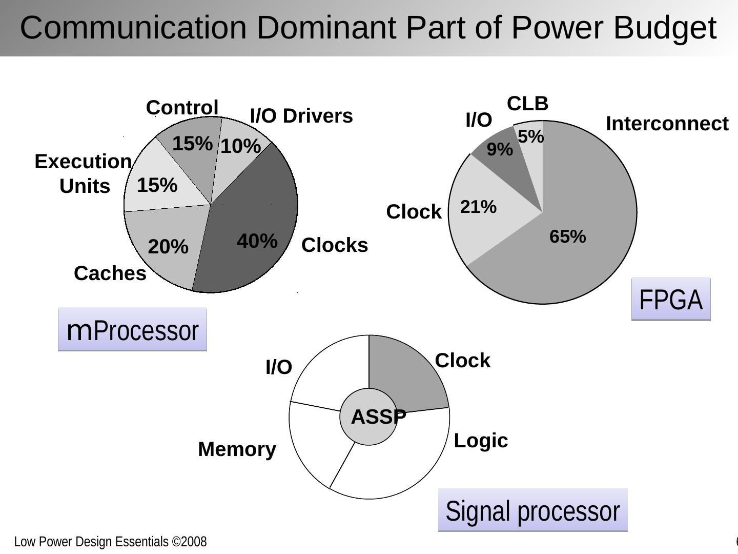
5 .Communication Dominant Part of Power Budget 65% 21% 9% 5% Interconnect Clock I/O CLB FPGA m Processor Signal processor Clock Logic Memory I/O Clocks Caches Execution Units Control I/O Drivers 40% 20% 15% 15% 10%
6 .Idealized Wire Scaling Model Parameter Relation Local Wire Constant Length Global Wire W, H, t 1/ S 1/ S 1/ S L 1/ S 1 1/ S C C LW/ t 1/ S 1 1/ S C R L / WH S S 2 S 2 /S C t p ~ CR L 2 / Ht 1 S 2 S 2 /S C 2 E CV 2 1/ SU 2 1/ U 2 1/( S C U 2 )
7 .Distribution of Wire Lengths on Chip [Ref: J. Davis, C&S’98] © IEEE 1998
8 .Technology Innovations Reduce dielectric permittivity (e.g. Aerogels or air) Reduce resistivity (e.g. Copper) Reduce wirelengths through 3D-integration Novel interconnect media (carbon nanotubes, optical) (Pictures courtesy of IBM and IFC FCRP) © IEEE 1998
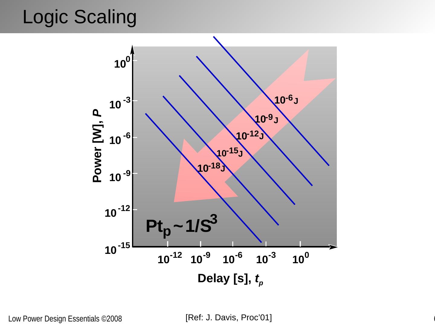
9 .Logic Scaling 10 -12 10 -9 10 -6 10 -3 10 0 Pt p ~ 1/S 3 10 0 10 -3 10 -6 10 -9 10 -12 10 -15 Power [W], P Delay [s], t p 10 -6 J 10 -9 J 10 -12 J 10 -15 J 10 -18 J [Ref: J. Davis, Proc’01]
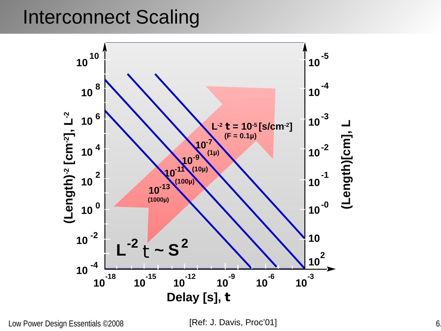
10 .Interconnect Scaling Delay [s], t (Length) -2 [cm -2 ], L -2 (Length)[cm], L 10 -18 10 -15 10 -12 10 -9 10 -6 10 -3 L -2 t = 10 -5 [s/cm -2 ] (F = 0.1µ) L -2 t ~ S 2 10 10 10 8 10 6 10 4 10 2 10 0 10 -2 10 -4 10 -5 10 -4 10 -3 10 -2 10 -1 10 -0 10 10 2 10 -13 (1000µ) 10 -11 (100µ) 10 -9 (10µ) 10 -7 (1µ) [Ref: J. Davis, Proc’01]
11 .Lower Bounds on Interconnect Energy Claude Shannon C: capacity in bits/sec B: bandwidth P s: average signal power Valid for an “infinitely long” bit transition (C/B→0) Equals 4.10 -21 J/bit at room temperature Shannon’s theorem on maximum capacity of communication channel [Ref: J. Davis, Proc’01]
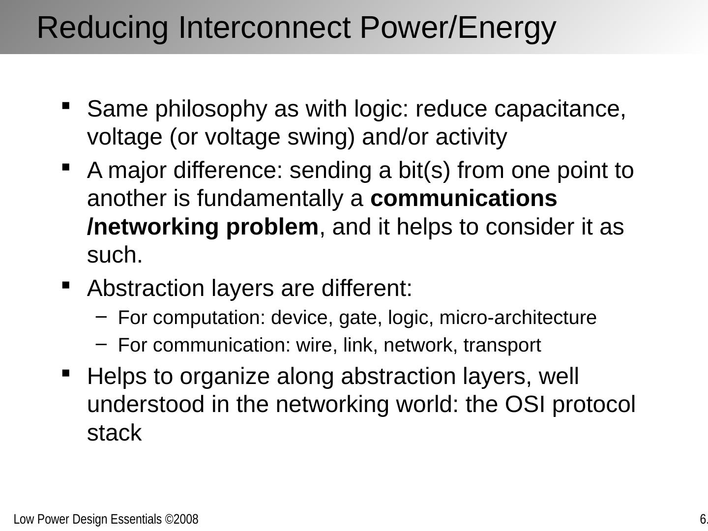
12 .Reducing Interconnect Power/Energy Same philosophy as with logic: reduce capacitance, voltage (or voltage swing) and/or activity A major difference: sending a bit(s) from one point to another is fundamentally a communications /networking problem , and it helps to consider it as such. Abstraction layers are different: For computation: device, gate, logic, micro-architecture For communication: wire, link, network, transport Helps to organize along abstraction layers, well understood in the networking world: the OSI protocol stack
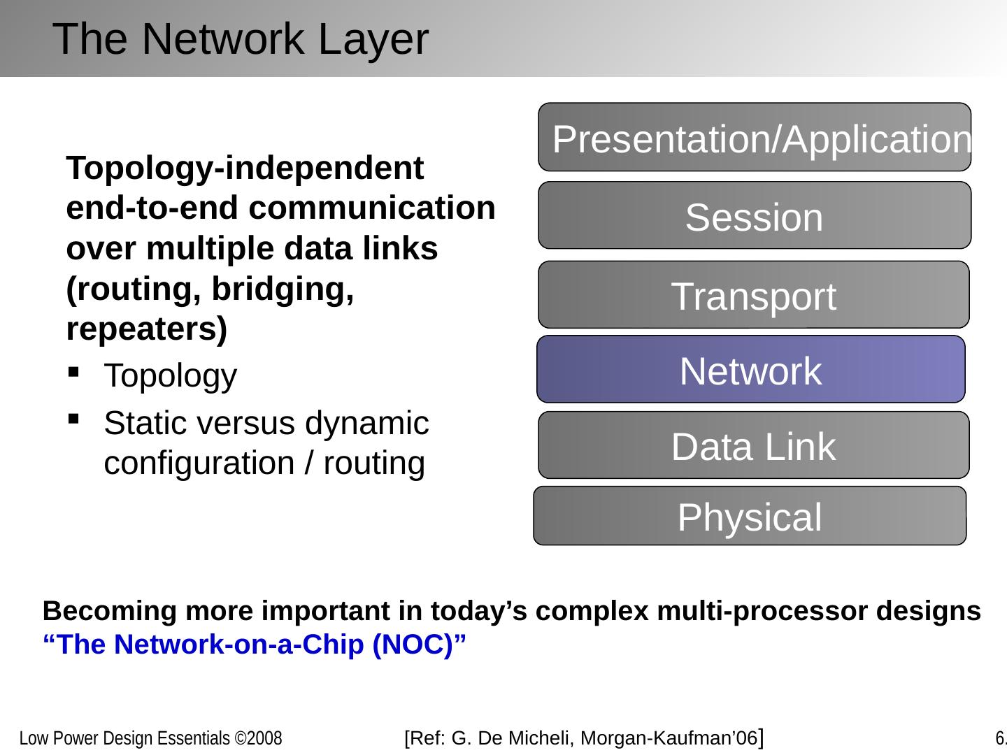
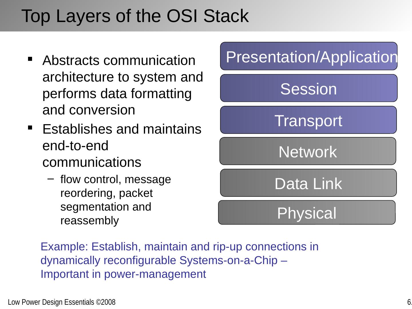
13 .OSI Protocol Stack Reference model for wired and wireless protocol design — Also useful guide for conception and optimization of on-chip communication Layered approach allows for orthogonalization of concerns and decomposition of constraints Network Transport Session Data Link Physical Presentation/Application No requirement to implement all layers of the stack Layered structure must not necessarily be maintained in final implementation [Ref: M. Sgroi , DAC’01]
14 .The Physical Layer Transmit bits over physical interconnect medium (wire) Physical medium Material choice, repeater insertion Signal waveform Discrete levels, pulses, modulated sinusoids Voltages Reduced swing Timing, synchronization Network Transport Session Data Link Physical Presentation/Application So far, on-chip communication almost uniquely “level-based”
15 .Repeater Insertion Optimal receiver insertion results in wire delay linear with L with R d C d and r w c w intrinsic delays of inverter and wire, respectively But: At major energy cost!
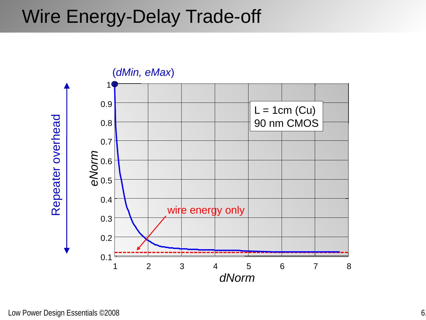
16 .Repeater Insertion ─ Example 1 cm Cu wire in 90 nm technology (on intermediate layers) r w = 250 W /mm; c w = 200 fF /mm t p = 0.69 r w c w L 2 = 3.45 nsec Optimal driver insertion: t popt = 0.5 nsec Requires insertion of 13 repeaters Energy per transition 8 times larger than just charging the wire (6 pJ verus 0.75 pJ )! It pays to back off!
17 .Wire Energy-Delay Trade-off 1 2 3 4 5 6 7 8 0.1 0.2 0.3 0.4 0.5 0.6 0.7 0.8 0.9 1 dNorm eNorm wire energy only L = 1cm (Cu) 90 nm CMOS ( dMin , eMax ) Repeater overhead
18 .Multi-dimensional Optimization Design parameters: Voltage, number of stages, buffer sizes Voltage scaling has largest impact, followed by selection of number of repeaters Transistor sizing secondary. 1 2 3 4 5 6 7 8 0 2 4 6 8 10 12 dNorm Number of stages 0.5 0.6 0.7 0.8 0.9 1 1.1 1.2 V DD (V)
19 .Reduced Swing E bit = CV DD V swing Concerns: Overhead (area, delay) Robustness (supply noise, crosstalk, process variations) Repeaters? Transmitter (TX) Receiver (RX)
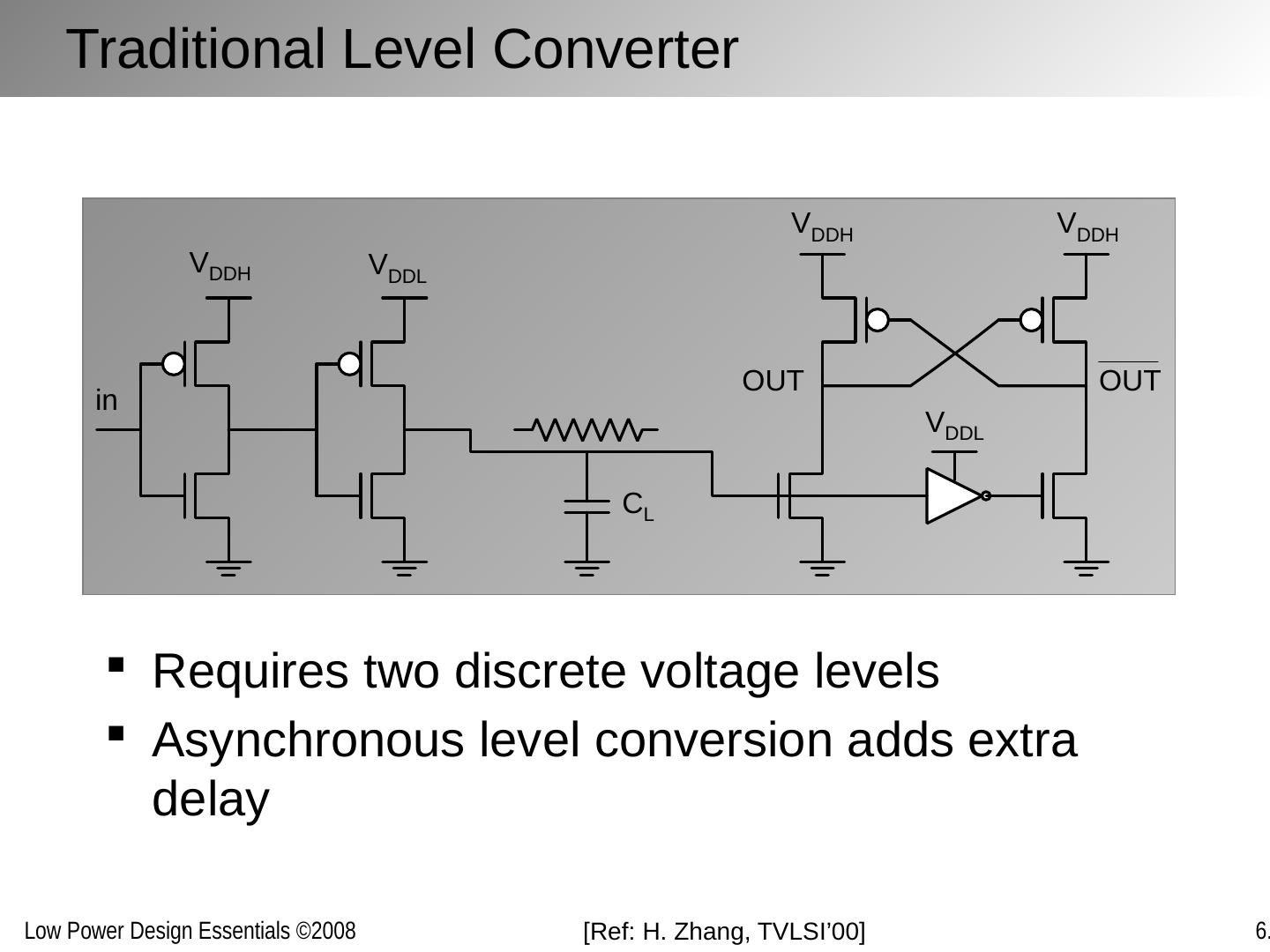
20 .Traditional Level Converter Requires two discrete voltage levels Asynchronous level conversion adds extra delay [Ref: H. Zhang, TVLSI’00]
21 .Avoiding Extra References [Ref: H. Zhang, VLSI’00] VTC Transient
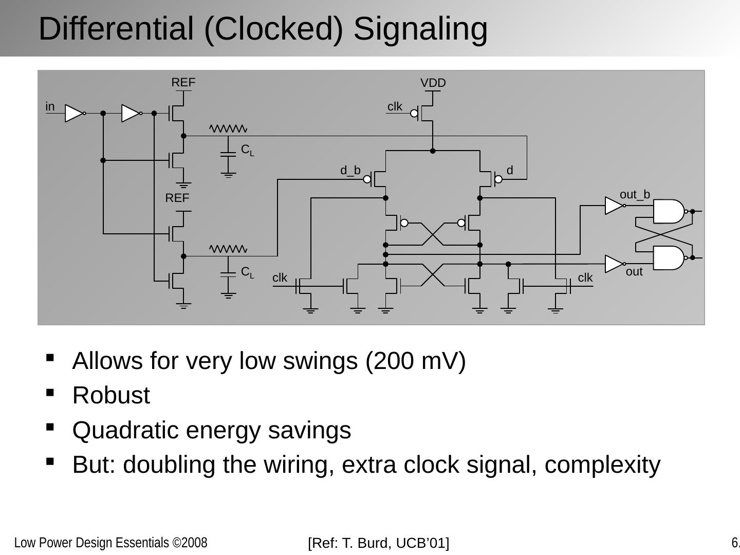
22 .Differential (Clocked) Signaling Allows for very low swings (200 mV) Robust Quadratic energy savings But: doubling the wiring, extra clock signal, complexity [Ref: T. Burd , UCB’01]
23 .Lower Bound on Signal Swing? Reduction of signal swing translates into higher power dissipation in receiver – trade-off between wire and receiver energy dissipation Reduced SNR impacts reliability – current on-chip interconnect strategies require Bit Error Rate (BER) of zero (in contrast to communication and network links) Noise source: power supply noise, crosstalk Swings as low as 200 mV have been reported [Ref: Burd’00], 100 mV definitely possible Further reduction requires crosstalk suppression shielding folding GND GND GND
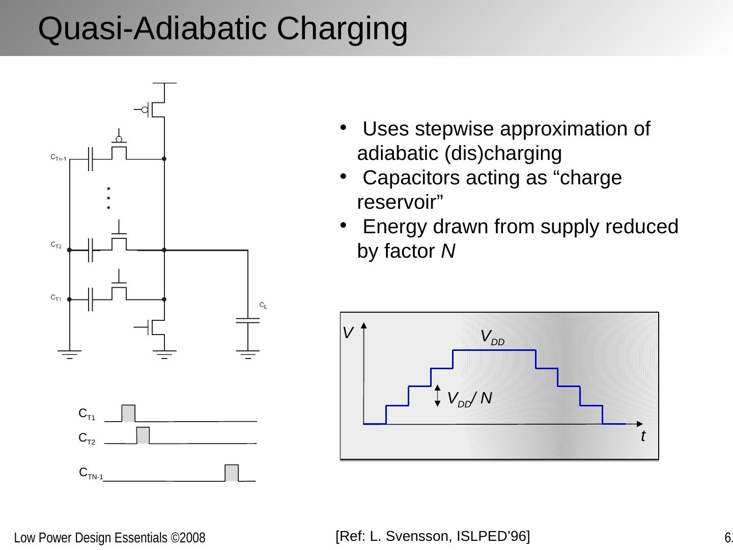
24 .Quasi-Adiabatic Charging t V V DD V DD / N [Ref: L. Svensson , ISLPED’96] Uses stepwise approximation of adiabatic ( dis )charging Capacitors acting as “charge reservoir” Energy drawn from supply reduced by factor N C T1 C T2 C TN-1
25 .Charge Redistribution Schemes V DD / 2 V DD / 4 3V DD / 4 Precharge Eval Precharge B 0 B 0 B 1 B 1 B 0 = 0 B 1 = 1 V DD E E E P P GND RX1 RX0 1 0 B1 B1 B0 B0 Charge recycled from top to bottom Precharge phase equalizes differential lines Energy/bit = 2 C ( V DD / N ) 2 Challenges: Receiver design, noise margins [Ref: H. Yamauchi, JSSC’95]
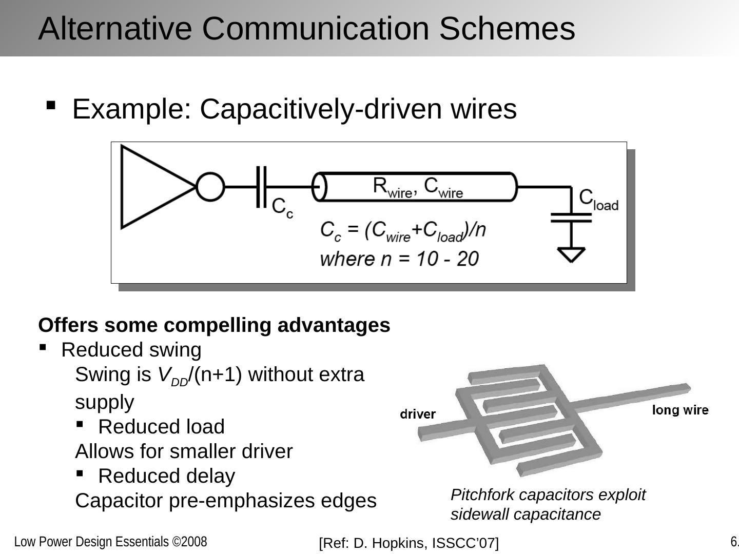
26 .Alternative Communication Schemes Example: Capacitively-driven wires Offers some compelling advantages Reduced swing Swing is V DD /(n+1) without extra supply Reduced load Allows for smaller driver Reduced delay Capacitor pre-emphasizes edges Pitchfork capacitors exploit sidewall capacitance [Ref: D. Hopkins, ISSCC’07]
27 .Signaling Protocols Network Processor Module ( m Proc , ALU, MPY, SRAM…) d in req in ack in d out req out ack out D in REQ in done Globally Asynchronous self-timed handshaking protocol Allows individual modules to dynamically trade-off performance for energy-efficiency
28 .Signaling Protocols Network Physical Layer Interface Module Processor Module ( mProc , ALU , MPY, SRAM…) d in req in ack in d out req out ack out d in d out clk D in REQ in Clk done Locally synchronous done Globally Asynchronous
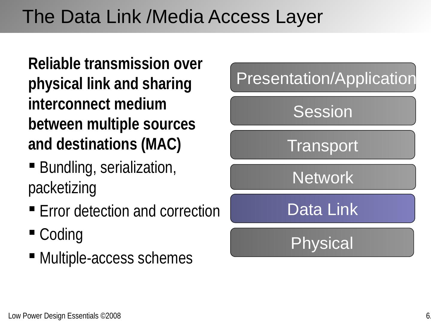
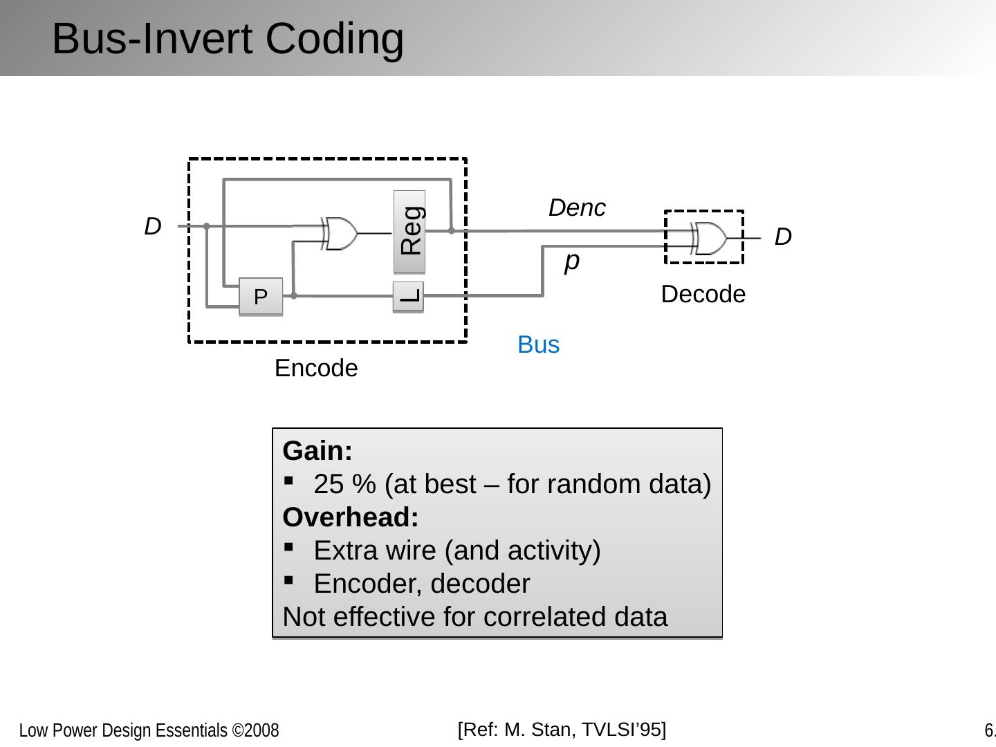
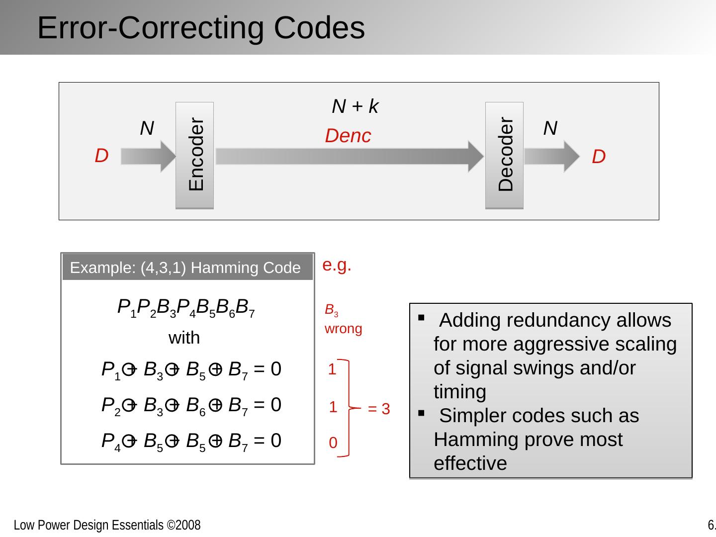
29 .The Data Link /Media Access Layer Reliable transmission over physical link and sharing interconnect medium between multiple sources and destinations (MAC) Bundling, serialization, packetizing Error detection and correction Coding Multiple-access schemes Network Transport Session Data Link Physical Presentation/Application


