- 快召唤伙伴们来围观吧
- 微博 QQ QQ空间 贴吧
- 文档嵌入链接
- 复制
- 微信扫一扫分享
- 已成功复制到剪贴板
金属氧化物半导体场效应晶体管
展开查看详情
1 . Lecture #24 ANNOUNCEMENT • Special session (led by the TA’s): – MEDICI demonstration (for Part II of Design Project) – 3-4 PM, Friday April 18, 521 Cory (Hogan Room) OUTLINE The MOSFET (cont.) • Theory of Operation • Long-channel I-V (Square-Law Theory) (Reading: Textbook Chapter 17.2) Spring 2003 EE130 Lecture 24, Slide 1 Bias-Temperature Stress Measurement Used to determine mobile charge density in MOS dielectric (units: C/cm2) Na+ located at lower SiO2 interface ∆VFB Æ reduces VFB Na+ located at upper SiO2 interface Æ no effect on VFB Positive oxide charge shifts the flatband voltage in the negative direction: tox QF 1 QIT (ψ s ) VFB = φ MS − − Cox ε SiO2 ∫ xρ 0 ox ( x )dx − Cox QM = −Cox ∆VFB Spring 2003 EE130 Lecture 24, Slide 2 1
2 . Clarification: Effect of Interface Traps “Donor-like” traps are charge-neutral when (a) (c) filled, positively charged (b) when empty Positive oxide charge causes C-V curve to (a) shift toward left (b) (more shift as VG decreases) Traps cause “sloppy” C-V and also (c) greatly degrade mobility in channel Q (ψ ) ∆VG = − IT s Cox Spring 2003 EE130 Lecture 24, Slide 3 NMOSFET Operation (Qualitative) VGS < VT: depletion layer VGS > VT : VDS ≈ 0 I DS = WQinv v = WQ inv µeff E VDS > 0 V = WQ inv µeff DS L Spring 2003 EE130 Lecture 24, Slide 4 2
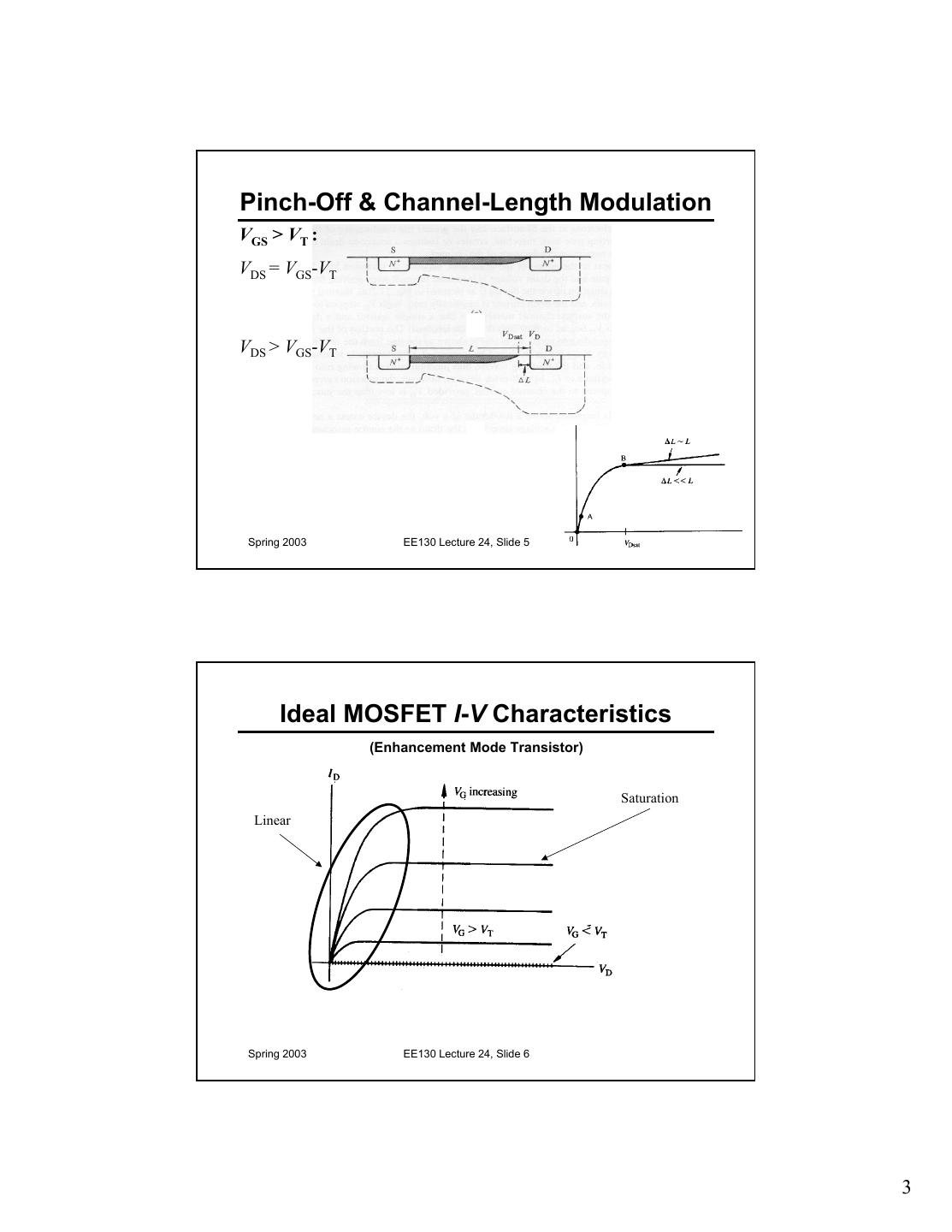
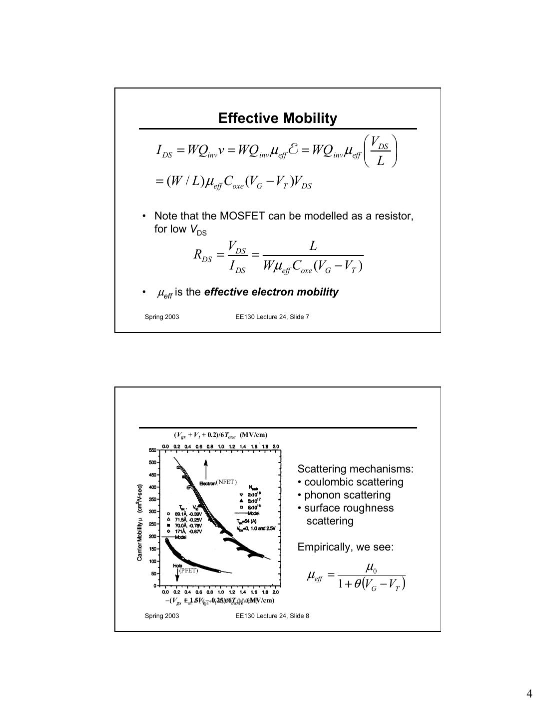
3 .Pinch-Off & Channel-Length Modulation VGS > VT : VDS = VGS-VT VDS > VGS-VT Spring 2003 EE130 Lecture 24, Slide 5 Ideal MOSFET I-V Characteristics (Enhancement Mode Transistor) Saturation Linear Spring 2003 EE130 Lecture 24, Slide 6 3
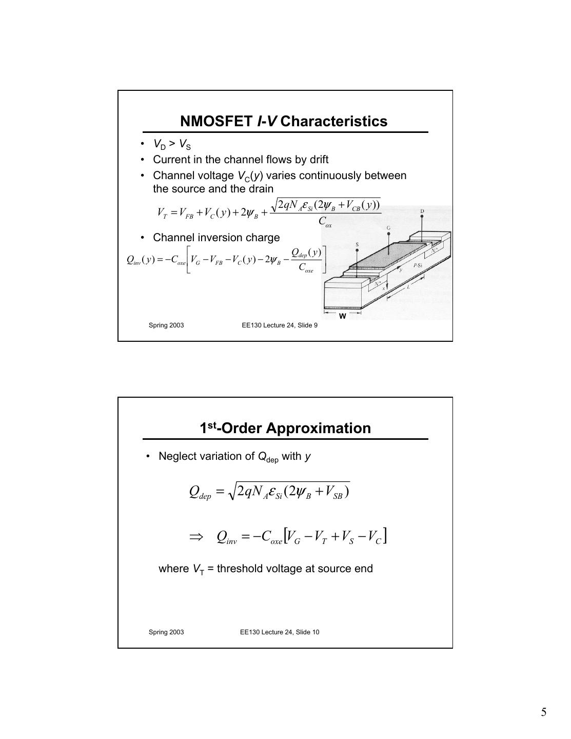
4 . Effective Mobility V I DS = WQinv v = WQ inv µeff E = WQ inv µeff DS L = (W / L) µeff Coxe (VG − VT )VDS • Note that the MOSFET can be modelled as a resistor, for low VDS VDS L RDS = = I DS Wµeff Coxe (VG − VT ) • µeff is the effective electron mobility Spring 2003 EE130 Lecture 24, Slide 7 (Vgs + V t + 0.2)/6Toxe (MV/cm) Scattering mechanisms: (NFET) • coulombic scattering • phonon scattering • surface roughness scattering Empirically, we see: µ0 (PFET) µeff = 1 + θ (VG − VT ) –(Vgs + 1.5V t – 0.25)/6Tox e (MV/cm) Spring 2003 EE130 Lecture 24, Slide 8 4
5 . NMOSFET I-V Characteristics • VD > VS • Current in the channel flows by drift • Channel voltage VC(y) varies continuously between the source and the drain 2qN Aε Si ( 2ψ B + VCB ( y )) VT = VFB + VC ( y ) + 2ψ B + Cox • Channel inversion charge Q ( y) Qinv ( y ) = −Coxe VG − VFB − VC ( y ) − 2ψ B − dep Coxe W Spring 2003 EE130 Lecture 24, Slide 9 1st-Order Approximation • Neglect variation of Qdep with y Qdep = 2qN Aε Si (2ψ B + VSB ) ⇒ Qinv = −Coxe [VG − VT + VS − VC ] where VT = threshold voltage at source end Spring 2003 EE130 Lecture 24, Slide 10 5
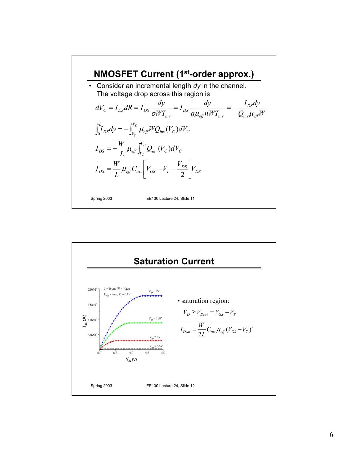
6 . NMOSFET Current (1st-order approx.) • Consider an incremental length dy in the channel. The voltage drop across this region is dy dy I dy dVC = I DS dR = I DS = I DS = − DS σWTinv qµeff nWTinv Qinv µeff W L VD ∫I 0 DS dy = − ∫ µeff WQinv (VC )dVC VS W VD I DS = − µeff ∫ Qinv (VC )dVC L VS W V I DS = µeff Coxe VGS − VT − DS VDS L 2 Spring 2003 EE130 Lecture 24, Slide 11 Saturation Current • saturation region: VD ≥ VDsat = VGS − VT W I Dsat = Coxe µeff (VGS − VT ) 2 2L Spring 2003 EE130 Lecture 24, Slide 12 6


