- 快召唤伙伴们来围观吧
- 微博 QQ QQ空间 贴吧
- 文档嵌入链接
- 复制
- 微信扫一扫分享
- 已成功复制到剪贴板
CMOS工艺与MOSFET结构
展开查看详情
1 . Lecture #28 ANNOUNCEMENTS • Quiz #6 next Thursday (May 8) – Topics covered: MOSFET – Closed book; calculator, 6 pages of notes allowed OUTLINE – MOSFET scaling – CMOS technology – Silicon on Insulator technology Reading: Reader Part III, Chapter 4 Spring 2003 EE130 Lecture 28, Slide 1 Short-Channel MOSFET VT • For short-channel MOSFETs, VT is usually defined as the gate voltage at which the maximum barrier for electrons at the surface equals 2ψB. This is lower than the long-channel VT by an amount 24Toxe ∆VT = ψ bi (ψ bi + VDS )e −πL / 2(Wdm +3Toxe ) Wdm EG where ψ bi = +ψ B 2q Note: This equation assumes that rj > Wdm Î To minimize VT roll-off, Nbody should be high enough to ensure that Lmin > 2Wdm Spring 2003 EE130 Lecture 28, Slide 2 1
2 . Constant-Field Scaling • Voltages and MOSFET dimensions are scaled by the same factor κ>1, so that the electric field remains unchanged Spring 2003 EE130 Lecture 28, Slide 3 Constant-Field Scaling (cont.) • Circuit speed improves by κ • Power dissipation per function is reduced by κ2 Spring 2003 EE130 Lecture 28, Slide 4 2
3 . VT Design Trade-Off • Low VT is desirable for high ON current: Idsat ∝ (Vdd - Vt)η 1 < η < 1.5 • But VT is needed for low OFF current: log IDS • Non-scaling factors: Low VT • kT/q High VT • EG IOFF,low VT • Tinv ÆVT cannot be scaled IOFF,high VT aggressively! 0 VGS Spring 2003 EE130 Lecture 28, Slide 5 • Since VT cannot be scaled down aggressively, the power-supply voltage (VDD) has not been scaled down in proportion to the MOSFET channel length Spring 2003 EE130 Lecture 28, Slide 6 3
4 . Generalized Scaling • Electric field intensity increases by a factor α>1 • Nbody must be scaled up by α to control short-channel effects • Reliability and power density are issues Spring 2003 EE130 Lecture 28, Slide 7 CMOS Technology Both n-channel and p-channel MOSFETs are fabricated on the same chip (VTp = -VTn ) • Primary advantage: – Lower average power dissipation • In steady state, either the NMOS or PMOS device is off, so there is no d.c. current path between VDD and GND • Disadvantages: – More complex (expensive) process – Latch-up problem Spring 2003 EE130 Lecture 28, Slide 8 4
5 .Need p-regions (for NMOS) and n-regions (for PMOS) on the wafer surface, e.g.: Single-well technology NA ND • n-well must be deep enough n-well to avoid vertical punch-through p-substrate NA ND Twin-well technology p-well n-well • Wells must be deep enough to avoid vertical punch-through p- or n-substrate (lightly doped) Spring 2003 EE130 Lecture 28, Slide 9 CMOS Latch-up CMOS Inverter: Vin VDD VSS Vout n+ p+ p+ n+ n+ p+ n-well p-Si VDD Equivalent circuit: Vin Vout Spring 2003 EE130 Lecture 28, Slide 10 5
6 . Coupled parasitic npn and pnp bipolar transistors: If either BJT enters the active mode, the SCR will enter into the forward conducting mode (large current flowing between VDD and GND) if βnpnβpnp > 1 => circuit burnout! Latch-up is triggered by a transient increase in current, caused by • transient currents (ionizing radiation, impact ionization, etc.) • voltage transients • e.g. negative voltage spikes which forward-bias the pn junction momentarily Spring 2003 EE130 Lecture 28, Slide 11 How to Prevent CMOS Latchup 1. Reduce minority-carrier lifetimes in well/substrate 2. Use highly doped substrate or wells: (a) n-well p-epi Rsub p+-substrate β npn (b) n Rwell n+ p-sub βpnp “retrograde well” Spring 2003 EE130 Lecture 28, Slide 12 6
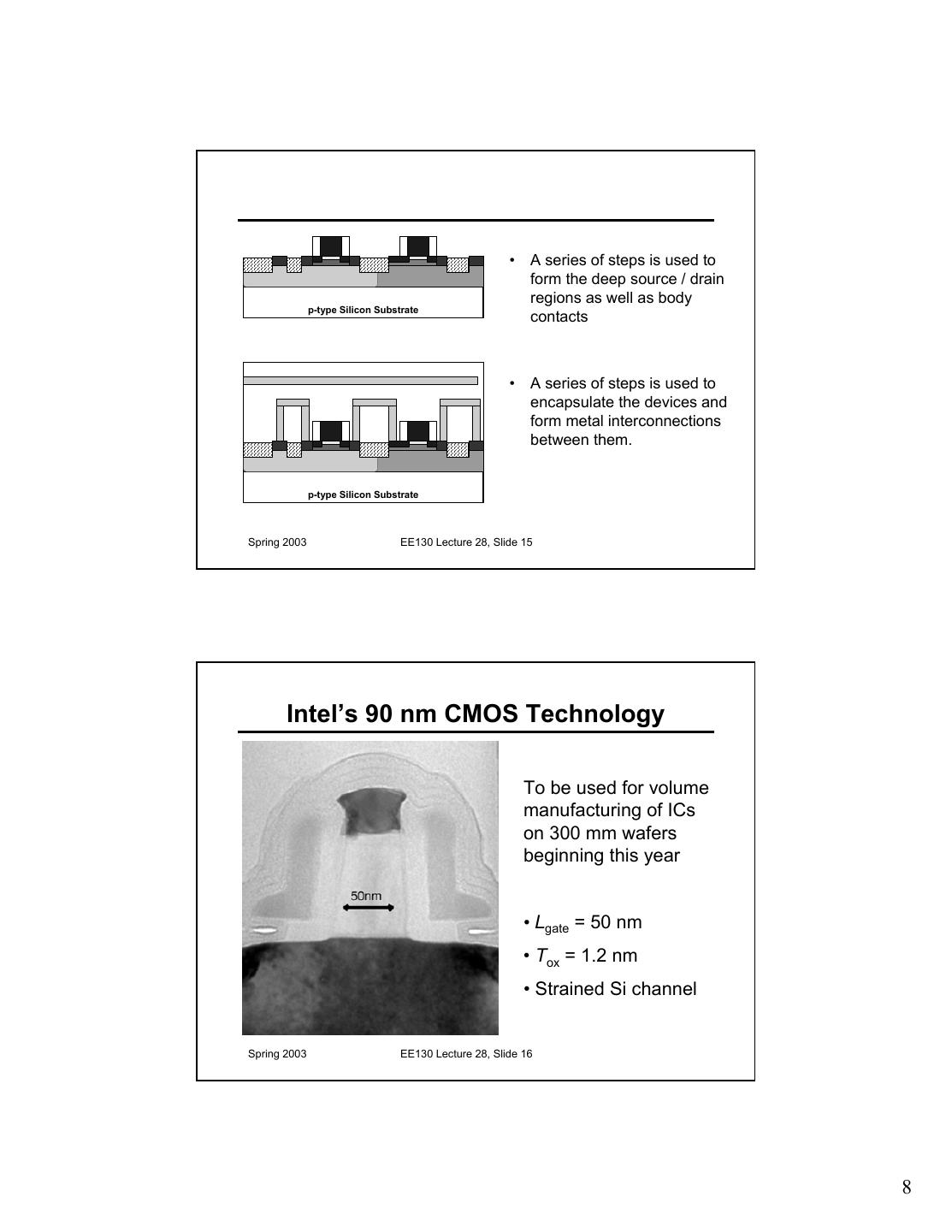
7 . Modern CMOS Fabrication Process p-type Silicon Substrate • A series of lithography, etch, Shallow Trench Isolation (STI) - oxide and fill steps are used to p-type Silicon Substrate create silicon islands isolated by oxide • Lithography and implant steps are used to set NMOS p-type Silicon Substrate and PMOS doping levels Spring 2003 EE130 Lecture 28, Slide 13 • A thin gate oxide is grown p-type Silicon Substrate • Poly-Si is deposited and patterned to form gate electrodes p-type Silicon Substrate • Lithography and implantation is used to form NLDD and p-type Silicon Substrate PLDD regions Spring 2003 EE130 Lecture 28, Slide 14 7
8 . • A series of steps is used to form the deep source / drain regions as well as body p-type Silicon Substrate contacts • A series of steps is used to encapsulate the devices and form metal interconnections between them. p-type Silicon Substrate Spring 2003 EE130 Lecture 28, Slide 15 Intel’s 90 nm CMOS Technology To be used for volume manufacturing of ICs on 300 mm wafers beginning this year • Lgate = 50 nm • Tox = 1.2 nm • Strained Si channel Spring 2003 EE130 Lecture 28, Slide 16 8
9 . Strained Si I Dsat ∝ v × Qinv Æ IDsat can be increased by enhancing field-effect mobilities, by straining the Si channel: Spring 2003 EE130 Lecture 28, Slide 17 Courtesy of J. Hoyt, MIT Mobility Enhancement with Strain Spring 2003 EE130 Lecture 28, Slide 18 9
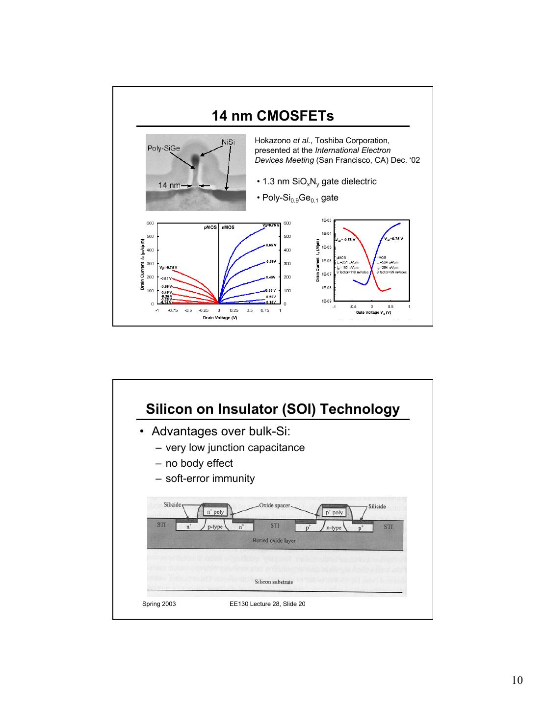
10 . 14 nm CMOSFETs Hokazono et al., Toshiba Corporation, presented at the International Electron Devices Meeting (San Francisco, CA) Dec. ‘02 • 1.3 nm SiOxNy gate dielectric • Poly-Si0.9Ge0.1 gate Spring 2003 EE130 Lecture 28, Slide 19 Silicon on Insulator (SOI) Technology • Advantages over bulk-Si: – very low junction capacitance – no body effect – soft-error immunity Spring 2003 EE130 Lecture 28, Slide 20 10


