- 快召唤伙伴们来围观吧
- 微博 QQ QQ空间 贴吧
- 文档嵌入链接
- 复制
- 微信扫一扫分享
- 已成功复制到剪贴板
备用内存优化
展开查看详情
1 .Optimizing Power @ Standby Memory
2 .Chapter Outline Memory in Standby Voltage Scaling Body Biasing Periphery
3 .Memory Dominates Processor Area SRAM is a major source of static power in ICs, especially for low power applications Special memory requirement: need to retain state in standby Metrics for standby: 1. Leakage power 2. Energy overhead for entering/leaving standby 3. Timing/area overhead BL BL WL M1 M2 M3 M4 M5 M6 Q QB
4 .Reminder of “Design Time” Leakage Reduction Design-time techniques (Ch 7) also impact leakage High V TH transistors Different precharge voltages Floating BLs This Chapter: adaptive methods that uniquely address memory standby power
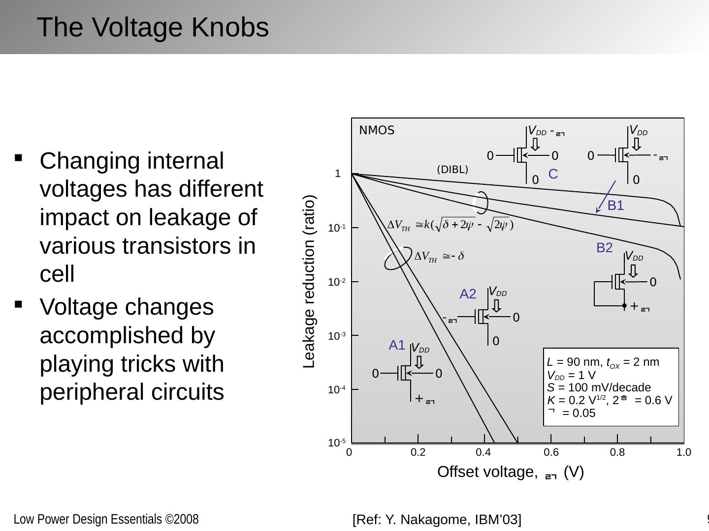
5 .The Voltage Knobs Changing internal voltages has different impact on leakage of various transistors in cell Voltage changes accomplished by playing tricks with peripheral circuits [Ref: Y. Nakagome , IBM’03 ] Offset voltage, (V) Leakage reduction (ratio) 1 10 -1 10 -2 10 -3 10 -4 0 0.2 0.4 0.6 0.8 1.0 10 -5 L = 90 nm, t OX = 2 nm V DD = 1 V S = 100 mV/decade K = 0.2 V 1/2 , 2 = 0.6 V = 0.05 V DD 0 0 - V DD 0 0 - V DD + 0 V DD - 0 0 0 (DIBL) NMOS V DD 0 0 + C B1 B2 A1 A2
6 .Lower V DD in Standby Basic Idea: Lower V DD lowers leakage sub-threshold leakage GIDL gate tunneling Question: What sets the lower limit? [Ref : K. Flautner , ISCA ’02] V DD V DDlow V DD _SRAM drowsy drowsy SRAM V DD V DDH V DDL Active mode Standby mode Example
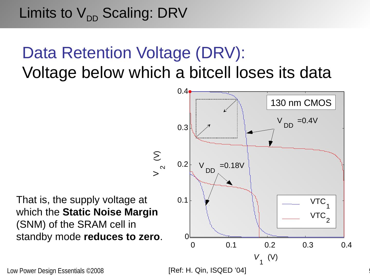
7 .Limits to V DD Scaling: DRV Data Retention Voltage (DRV): Voltage below which a bitcell loses its data That is, the supply voltage at which the Static Noise Margin (SNM) of the SRAM cell in standby mode reduces to zero . [Ref: H. Qin, ISQED ’04] 1 0 0.1 0.2 0.3 0.4 0 0.1 0.2 0.3 0.4 V (V) V 2 (V) VTC 1 VTC 2 V DD =0.18V V DD =0.4V 130 nm CMOS
8 .Power savings of DRV 0 0.2 0.4 0.6 0.8 1 0 10 20 30 40 50 60 Supply Voltage (V) Leakage Current (μA) Measured DRV range More than 90% reduction in leakage power with 350mV standby V DD (100mV guard band). Test chip in 130 nm CMOS technology with built-in voltage regulator 1.4 mm 1.4 mm IP Module of 4kB SRAM [Ref: H. Qin, ISQED’04]
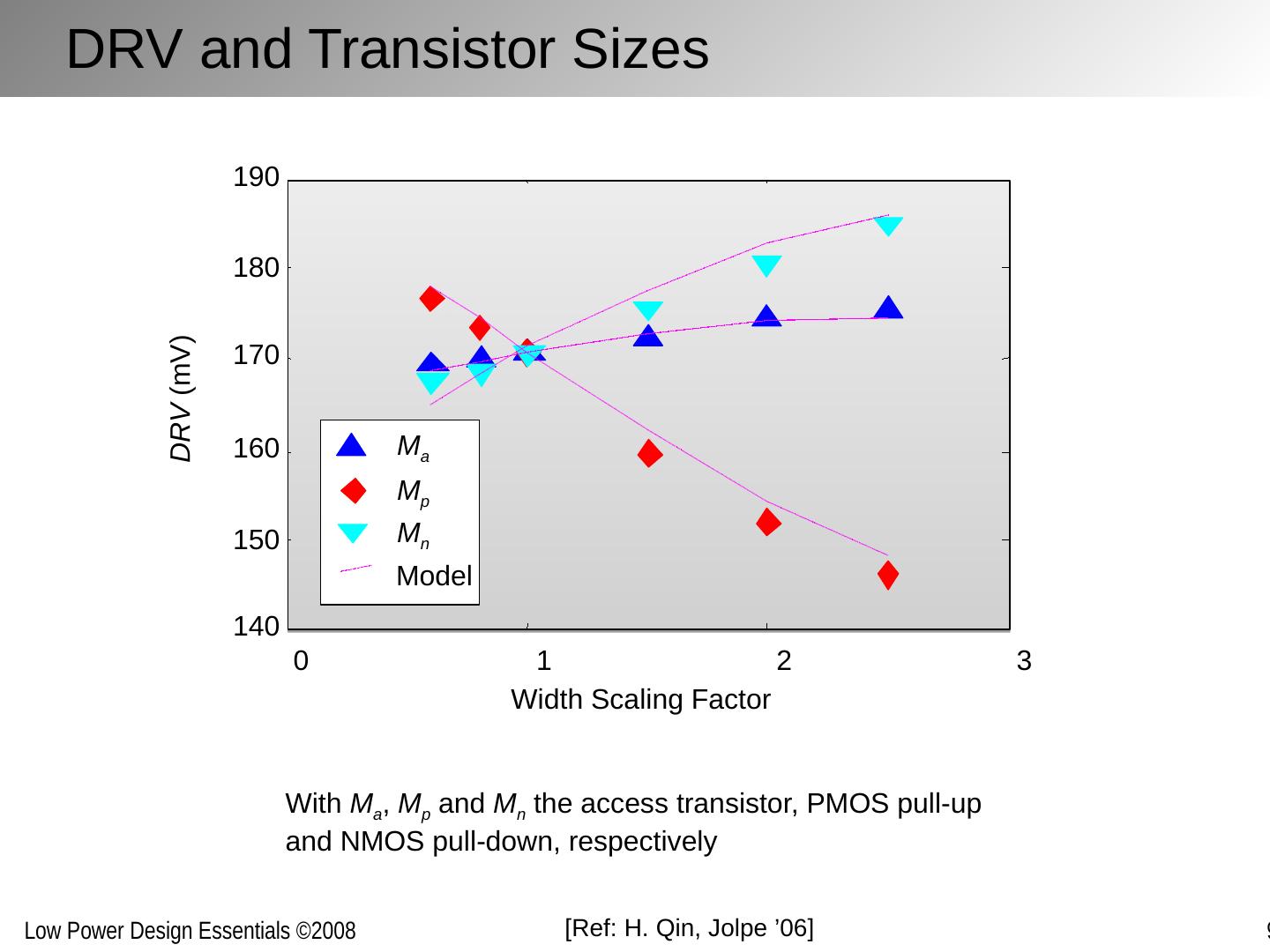
9 .DRV and Transistor Sizes 0 1 2 3 140 150 160 170 180 190 Width Scaling Factor DRV (mV) M a M p M n Model With M a , M p and M n the access transistor, PMOS pull-up and NMOS pull-down, respectively [Ref: H. Qin, Jolpe ’06]
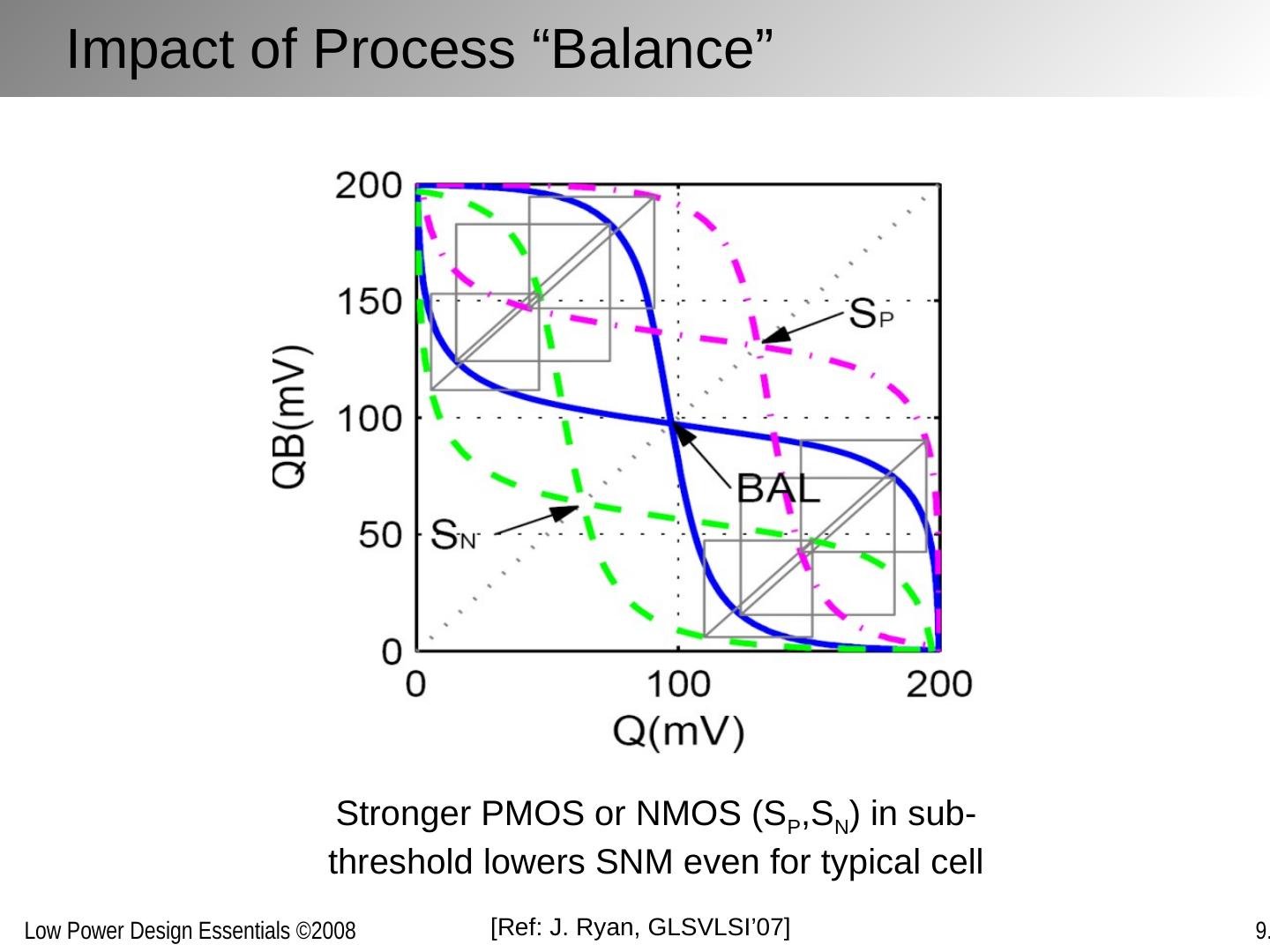
10 .Impact of Process “Balance” Stronger PMOS or NMOS (S P ,S N ) in sub-threshold lowers SNM even for typical cell [Ref: J. Ryan, GLSVLSI’07]
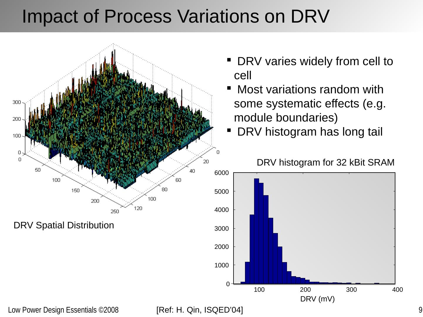
11 .Impact of Process Variations on DRV DRV Spatial Distribution DRV histogram for 32 kBit SRAM DRV varies widely from cell to cell Most variations random with some systematic effects (e.g. module boundaries) DRV histogram has long tail 130 nm CMOS [Ref: H. Qin, ISQED’04] 100 200 300 400 0 1000 2000 3000 4000 5000 6000 DRV (mV)
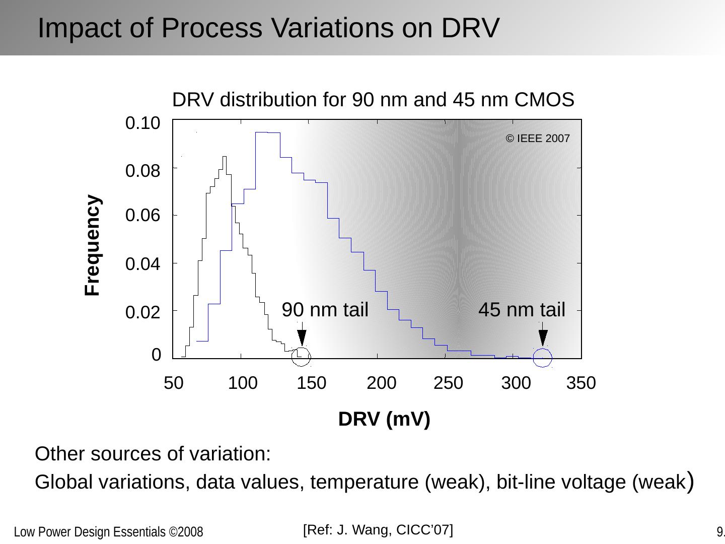
12 .Impact of Process Variations on DRV [Ref: J. Wang, CICC’07] DRV (mV) Frequency 50 100 150 200 250 300 350 45 nm tail 90 nm tail 0 0.02 0.04 0.06 0.08 0.10 Other sources of variation: Global variations, data values, temperature (weak), bit-line voltage (weak ) DRV distribution for 90 nm and 45 nm CMOS © IEEE 2007
13 .DRV Statistics for an Entire Memory DRV distribution is neither normal nor lognormal CDF model of DRV distribution ( F DRV ( x ) = 1- P ( SNM < 0, V DD = x )) [Ref: J. Wang, ESSCIRC 2007] Worst DRV (mV) Memory size s Model Normal LogNormal Monte-Carlo 3 4 5 6 7 8 100 350 3 00 250 2 00 150 © IEEE 2007
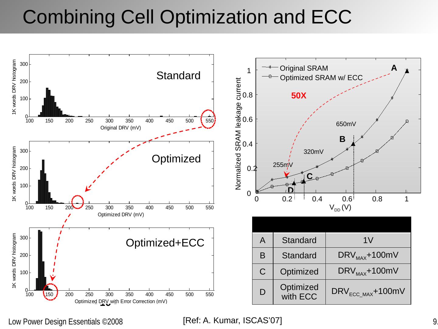
14 .100 200 300 400 0 1000 2000 3000 4000 5000 6000 DRV (mV) Reducing the DRV Chip DRV Cell optimization ECC (Error Correcting Codes) Cell optimization + ECC
15 .Lowering the DRV Using ECC Error Correction Challenges Maximize correction rate Minimize timing overhead Minimize area overhead Hamming [31, 26, 3] achieves 33% power saving Reed-Muller [256, 219, 8] achieves 35% power saving - 15 - Data P Write Read ECC Encoder ECC Decoder Data In Data Out SRAM with ECC D P Data Correction [Ref: A. Kumar, ISCAS’07]
16 .Combining Cell Optimization and ECC - 16 - A B C D 650mV 320mV 255mV 50X Standard Optimized Optimized+ECC 0 0.2 0.4 0.6 0.8 1 0 0.2 0.4 0.6 0.8 1 V DD (V) Normalized SRAM leakage current Original SRAM Optimized SRAM w/ ECC SRAM Standby V DD A Standard 1V B Standard DRV MAX +100mV C Optimized DRV MAX +100mV D Optimized with ECC DRV ECC_MAX +100mV [Ref: A. Kumar, ISCAS’07]
17 .How to Approach the DRV Safely? Core Cells Failure Detectors Sub-V T Controller V DD VCTRL voltages “1” “0” “1” “0” Adjustable Power Supply Reset Using “canary cells” to set the standby voltage in closed-loop [Ref: J. Wang, CICC’07]
18 .How to Approach the DRV Safely? Multiple sets of canary cells [Ref: J. Wang , CICC’07] 128Kb SRAM ARRAY Canary Replica & test circuit 0.6% area overhead in 90nm test chip Mean DRV of Canary Cells (V) More reliable Less power Failure Threshold SRAM cell DRV Histogram 0 0.2 0.4 0.6 0.8 VCTRL(V) 0 0.2 0.4 0.6 0.8 © IEEE 2007
19 .Raise bitcell V SS in standby (e.g. 0 to 0.5V) Lower BL voltage in standby (e.g. 1.5V to 1V) Raising V SS [Ref: K. Osada , JSSC’03] Lower voltage less gate leakage and GIDL ‘0’ is 0.5V Lower V DS less sub- V TH leakage (DIBL) Negative V BS reduces sub- V TH leakage 1.0V 1.0V WL=0V 1.5V 0.5V ‘0’ ‘1’
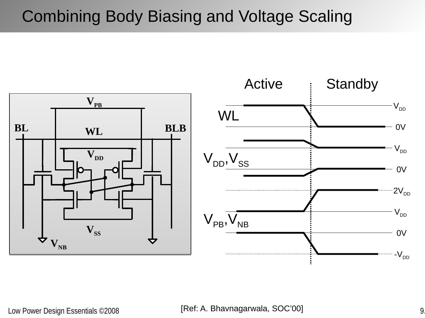
20 .Body Biasing Reverse Body Bias (RBB) for leakage reduction Move FET source (as in raised V SS ) Move FET body Example: Whenever WL is low, apply RBB 0V V DD 0V V DD 0V V DD 2V DD -V DD Active Standby WL V DD ,V SS V PB ,V NB BL BLB WL V DD V SS V PB V NB [Ref: H. Kawaguchi, VLSI Symp . 98]
21 .Combining Body Biasing and Voltage Scaling 0V V DD 0V V DD 0V V DD 2V DD -V DD Active Standby WL V DD ,V SS V PB ,V NB BL BLB WL V DD V SS V PB V NB [Ref: A. Bhavnagarwala , SOC’00]
22 .Combining Raised VSS and RBB 28X savings in standby power reported BL BLB WL V DD V SS [ Ref: L. Clark, TVLSI’04] V PB V NB Supply Active (V) Standby (V) V PB 1.0 1.75 V DD 1.0 1.0 V SS 0.0 0.65 V NB 0.0 0.0
23 .Voltage Scaling in and Around the Bitcell [1] K. Osada et al. JSSC 2001 [2] N. Kim et al. TVLSI 2004 [3] H. Qin et al. ISQED 2004 [4] K. Kanda et al. ASIC/SOC 2002 [5] A. Bhavnagarwala et al. SymVLSIC 2004 [6] T. Enomoto et al. JSSC 2003 [7] M. Yamaoka et al. SymVLSIC 2002 [8] M. Yamaoka et al. ISSC 2004 [9] A. Bhavnagarwala et al. ASIC/SOC 2000 [10] K. Itoh et al. SymVLSIC 1996 [11] H. Yamauchi et al. SymVLSIC 1996 [12] K. Osada et al. JSSC 2003 [13] K. Zhang et al. SymVLSIC 2004 [14] K. Nii et al. ISSCC 2004 [ 15] A. Agarwal et al. JSSC 2003 [ 16] K. Kanda et al. JSSC 2004 Voltage Approach Source(s) Bitcell V DD lower in active (e.g. DVS) lower in standby raise always raise for read access float or lower for write float for read access raise in standby [1] [2][3][4][5][6][7] [8][9] [5][9] [5][10] [10] Bitcell V SS raise in standby raise or float for write access lower for read access [6][7][11][12][13][14][15] [16] [9] Wordline (WL) negative for standby [4][10] WL driver V DD lower in standby [7] Well-biasing change with mode [4][9] Bitline V DD lower for standby [12] Large number of reported techniques
24 .Periphery Breakdown Periphery leakage often not ignorable Wide transistors to drive large load capacitors Low V TH transistors to meet performance specs Chapter 8 techniques for logic leakage reduction equally applicable, but … Task made easier than for generic logic because of well-defined structure and signal patterns of periphery e.g. decoders output 0 in standby Lower peripheral V DD can be used, but need fast level-conversion to interface with array
25 .Summary and Perspectives SRAM standby power is leakage dominated Voltage knobs are effective to lower power Adaptive schemes must account for variation to allow outlying cells to function Combined schemes are most promising e.g. Voltage scaling and ECC Important to assess overhead! Need for exploration and optimization framework, in the style we have defined for logic
26 .References Books and Book Chapters: K. Itoh , M. Horiguchi , and H. Tanaka, Ultra-Low Voltage Nano-Scale Memories , Springer 2007. T. Takahawara and K. Itoh , “Memory Leakage Reduction,” in Leakage in Nanometer CMOS Technologies , S. Narendra , Ed, Chapter 7, Springer 2006. Articles: A. Agarwal , L.Hai , K. Roy, “A single-V/sub t/ low-leakage gated-ground cache for deep submicron,” IEEE Journal of Solid State Circuits, pp. 319-328, Febr . 2003. A. Bhavnagarwala , A. Kapoor , A.; J. Meindl , “Dynamic-threshold CMOS SRAM cells for fast, portable applications,” Proceedings IEEE ASIC/SOC Conference, pp. 359-363, Sept. 2000. A. Bhavnagarwala et all, “A transregional CMOS SRAM with single, logic V/sub DD/ and dynamic power rails,” Proceedings IEEE VLSI Circuits Symposium, pp. 292-293, June 2004. L. Clark., M. Morrow, and W. Brown, “Reverse-body bias and supply collapse for low effective standby power,” IEEE Transactions on VLSI, pp. 947-956, Sep 2004. T. Enomoto , Y. Ota, and H. Shikano , “A self-controllable voltage level (SVL) circuit and its low-power high-speed CMOS circuit applications, “ IEEE Journal of Solid State Circuits, “ Vol. 38, Issue 7, pp. 1220-1226, July 2003. K. Flautner et al., “Drowsy Caches: Simple Techniques for Reducing Leakage Power., Proceedings ISCA 2002, pp. 148-157, Anchorage, May 2002. K. Itoh et al, “A deep sub-V, single power-supply SRAM cell with multi-VT, boosted storage node and dynamic load, Proceedings VLSI Circuits Symposium, pp. 132-133, June,1996. K. Kanda, T. Miyazaki, S. Min, H. Kawaguchi, T. Sakurai, “Two orders of magnitude leakage power reduction of low voltage SRAMs by row-by-row dynamic Vdd control (RRDV) scheme,” Proceedings IEEE ASIC/SOC Conference, pp. 381-385, Sept. 2002.
27 .References (cntd) K. Kanda, et al., “90% write power-saving SRAM using sense-amplifying memory cell,” IEEE Journal of Solid-State Circuits, pp.927 – 933, June 2004 H. Kawaguchi, Y. Itaka and T. Sakurai, “Dynamic Leakage Cut-off Scheme for Low-Voltage SRAMs,” Proceedings VLSI Symposium, pp. 140-141, June 1998. A. Kumar et al, “Fundamental Bounds on Power Reduction during Data-Retention in Standby SRAM,” Proceedings ISCAS 2007, pp. 1867-1870, May 2007. N.Kim , K. Flautner , D. Blaauw, and T. Mudge , “Circuit and microarchitectural techniques for reducing cache leakage power,” IEEE Transactions on VLSI, pp. 167-184, Feb 04 167-184 Y. Nakagome et al.. “Review and prospects of low-voltage RAM circuits,” IBM J. R & D, vol. 47. no. 516, pp. 525-552, Sep. /Nov. 2003. K. Osada , “Universal- Vdd 0.65-2.0-V 32-kB cache using a voltage-adapted timing-generation scheme and a lithographically symmetrical cell, “ IEEE Journal of Solid State Circuits, pp. 1738-1744, Nov. 2001. K. Osada et al, “16.7-fA/cell tunnel-leakage-suppressed 16-Mb SRAM for handling cosmic-ray-induced multierrors ,” IEEE Journal of Solid State Circuits, pp. 1952-1957, Nov. 2003. H. Qin, et al., “SRAM leakage suppression by minimizing standby supply voltage,” Proceedings ISQED, pp. 55-60, 2004. H. Qin, R. Vattikonda , T.Trinh , Y. Cao, and J. Rabaey, “SRAM Cell Optimization for Ultra-Low Power Standby,” Journal on Low Power Electronics, Vol. 2 No3, pp. 401–411, December 2006. J. Ryan, J. Wang, and B. Calhoun, "Analyzing and Modeling Process Balance for Sub-threshold Circuit Design“ Proceedings GLSVLSI, pp. 275-280, March 2007. J. Wang and B. Calhoun, "Canary Replica Feedback for Near-DRV Standby VDD Scaling in a 90nm SRAM“, Proceedings Custom Integrated Circuits Conference (CICC), pages 29-32, September 2007.
28 .References ( cntd ) J. Wang, A. Singhee , R. Rutenbar , and B. Calhoun, "Statistical Modeling for the Minimum Standby Supply Voltage of a Full SRAM Array“, Proceedings European Solid State Circuits Conference (ESSCIRC), pages 400-403, September 2007. M. Yamaoka et al. “0.4-V logic library friendly SRAM array using rectangular-diffusion cell and delta-boosted-array-voltage scheme, Proceedings VLSI Circuits Symposium, pp. 13-15, June 2002. M. Yamaoka, et al, “A 300MHz 25/ spl m A /Mb leakage on-chip SRAM module featuring process-variation immunity and low-leakage-active mode for mobile-phone application processor,” Proceedings IEEE Solid-State Circuits Conference, pp. 15-19, Febr 2004. K. Zhang et al., “SRAM design on 65nm CMOS technology with integrated leakage reduction scheme,” Proceedings VLSI Circuits Symposium, 2004, pp. 294-295, June 2004.


