- 快召唤伙伴们来围观吧
- 微博 QQ QQ空间 贴吧
- 文档嵌入链接
- 复制
- 微信扫一扫分享
- 已成功复制到剪贴板
纳米晶体管及其模型
展开查看详情
1 .Nanometer Transistors and Their Models
2 .Chapter Outline Nanometer transistor behavior and models Sub-threshold currents and leakage Variability Device and technology innovations
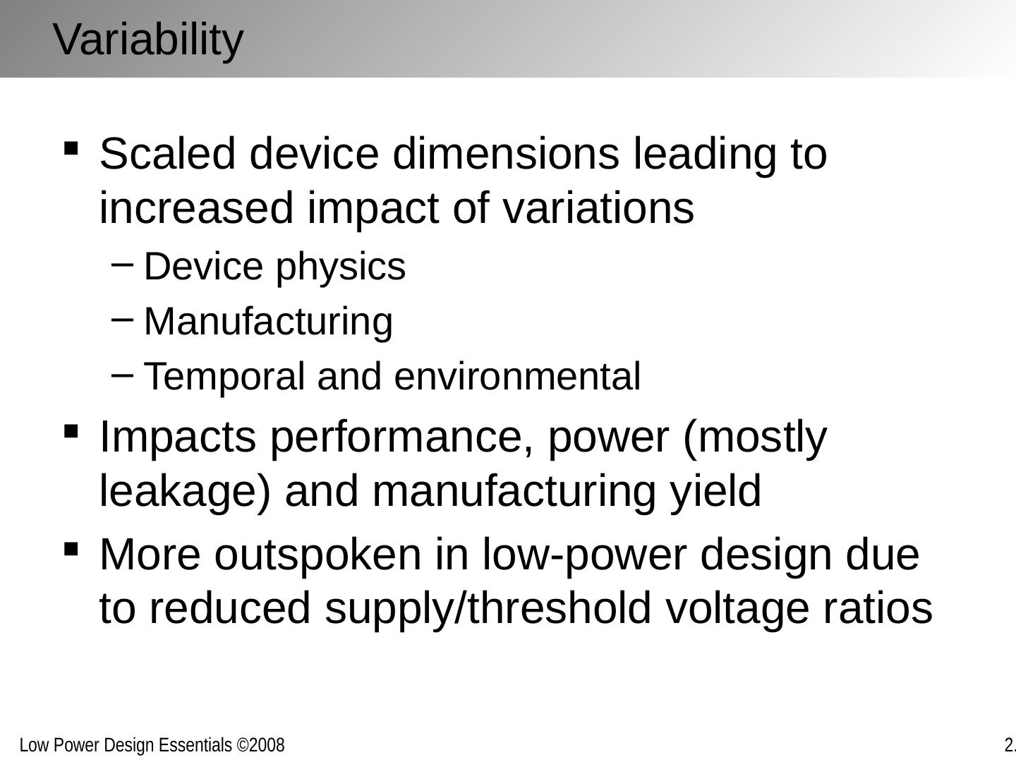
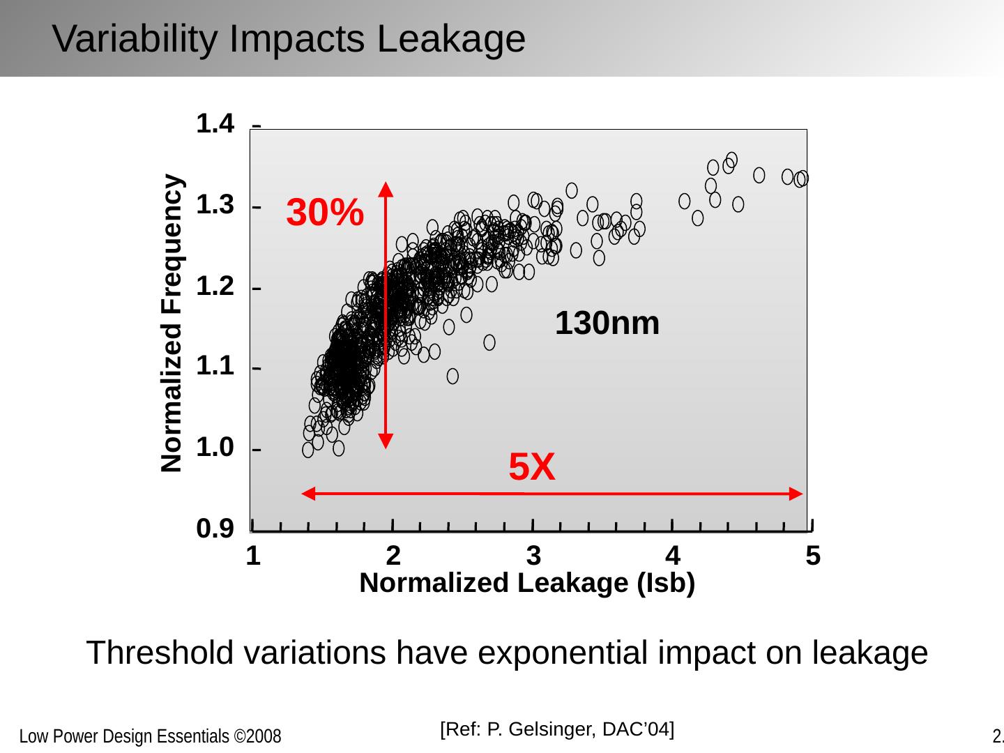
3 .Nanometer Transistors and Their Models Emerging devices in the sub-100 nm regime post challenges to low-power design Leakage Variability Reliability Yet also offer some opportunities Increased mobility Improved control (?) State-of-the-art low-power design should build on and exploit these properties Requires clear understanding and good models
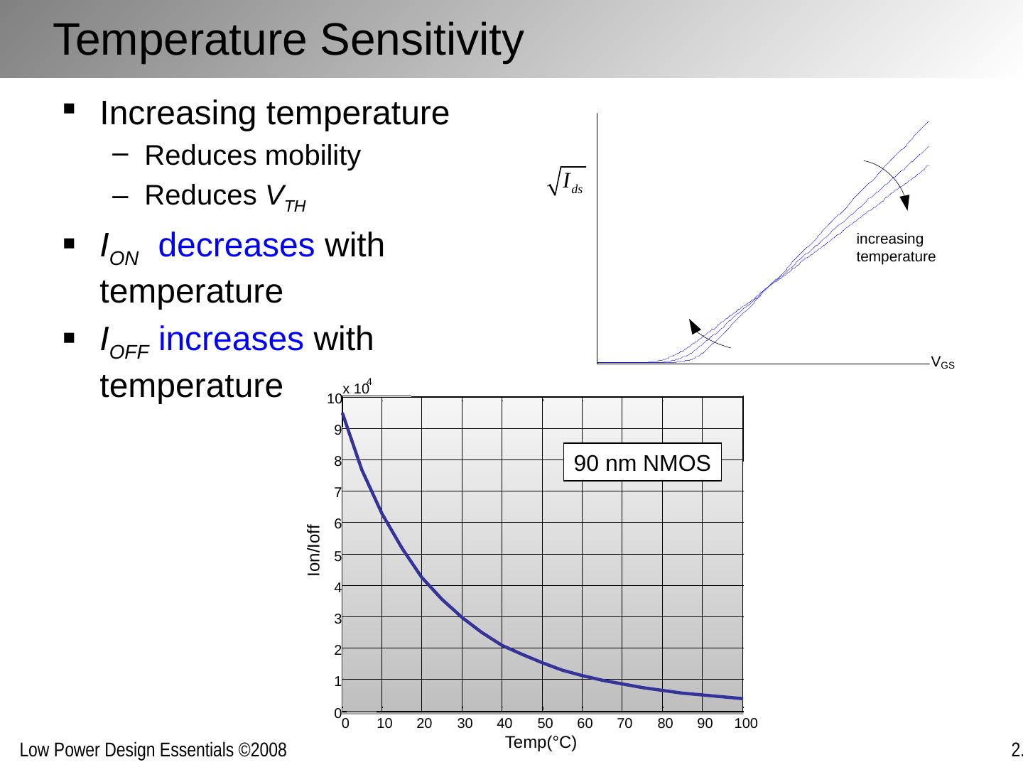
4 .The Sub-100 nm transistor Velocity-saturated Linear dependence between I D and V GS Threshold voltage V TH strongly impacted by channel length L and V DS Reduced threshold control through body biasing Leaky Subthreshold leakage Gate leakage → Decreasing I on over I off ratio
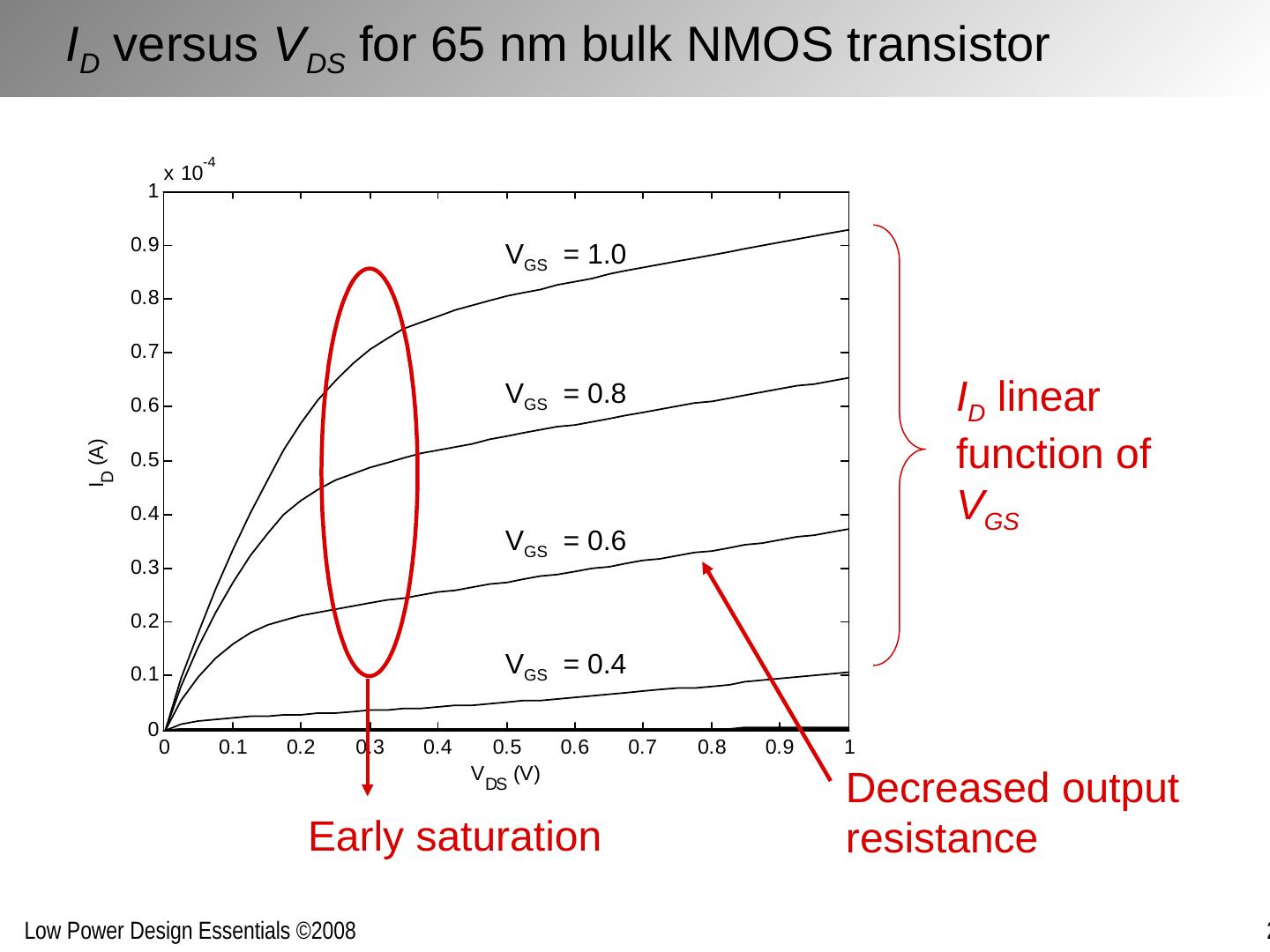
5 .I D versus V DS for 65 nm bulk NMOS transistor I D linear function of V GS V GS = 0.8 V GS = 0.6 V GS = 0.4 V GS = 1.0 Early saturation Decreased output resistance
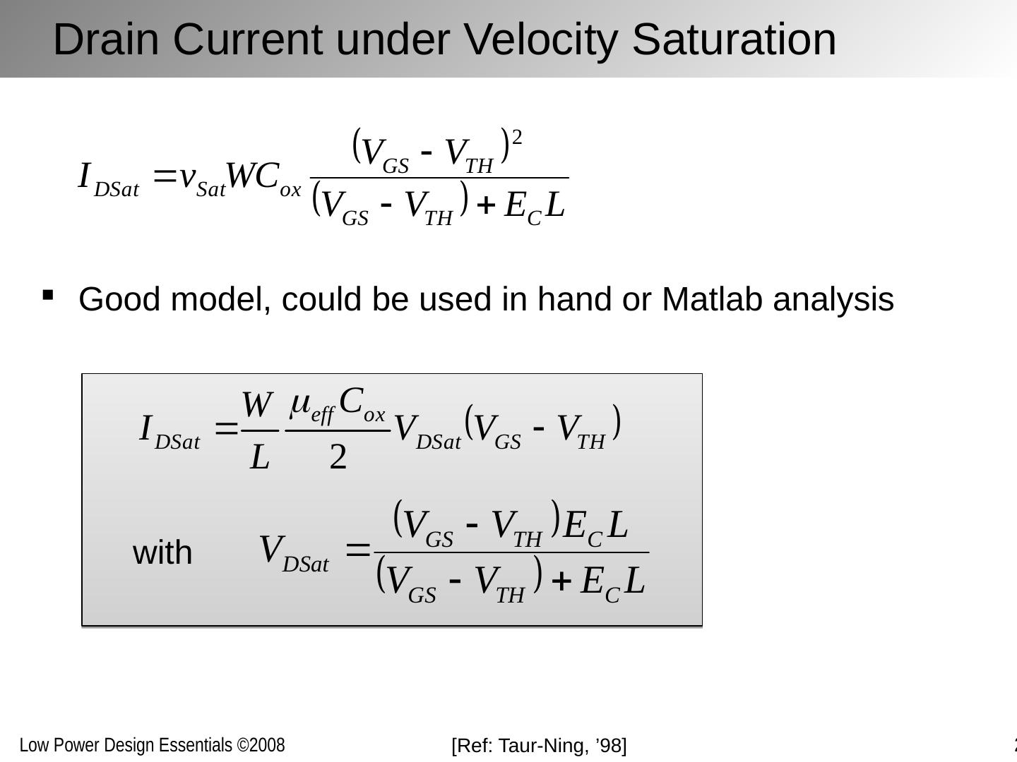
6 .Drain Current under Velocity Saturation Good model, could be used in hand or Matlab analysis with [Ref: Taur-Ning , ’98]
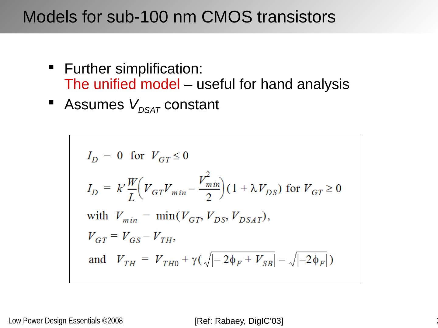
7 .Models for sub-100 nm CMOS transistors Further simplification: The unified model – useful for hand analysis Assumes V DSAT constant [Ref: Rabaey, DigIC’03]
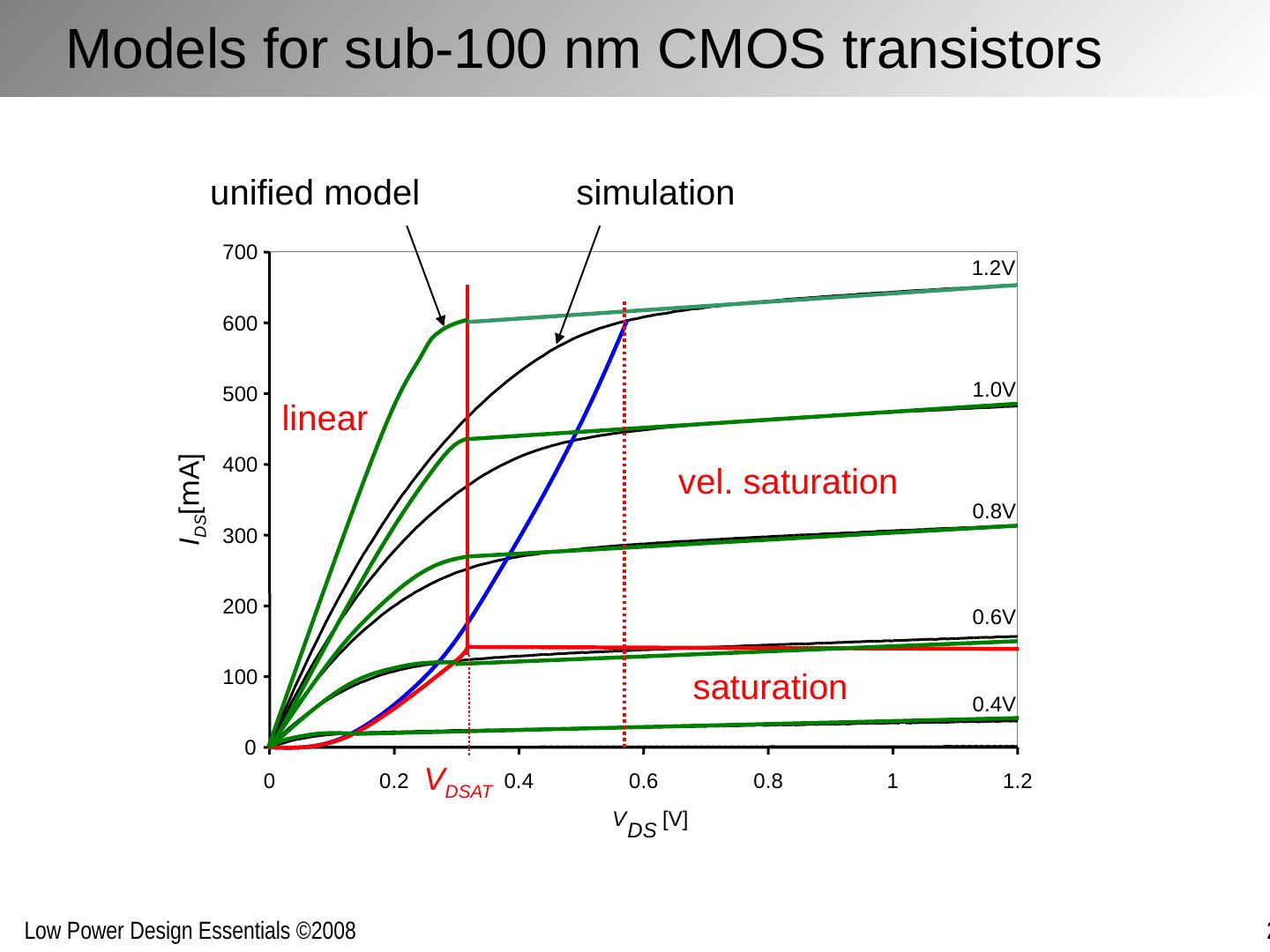
8 .Models for sub-100 nm CMOS transistors 0 100 200 300 400 500 600 700 0 0.2 0.4 0.6 0.8 1 1.2 V DS [V] 0.4V 0.6V 0.8V 1.0V 1.2V simulation unified model linear saturation vel. saturation V DSAT I DS [ m A]
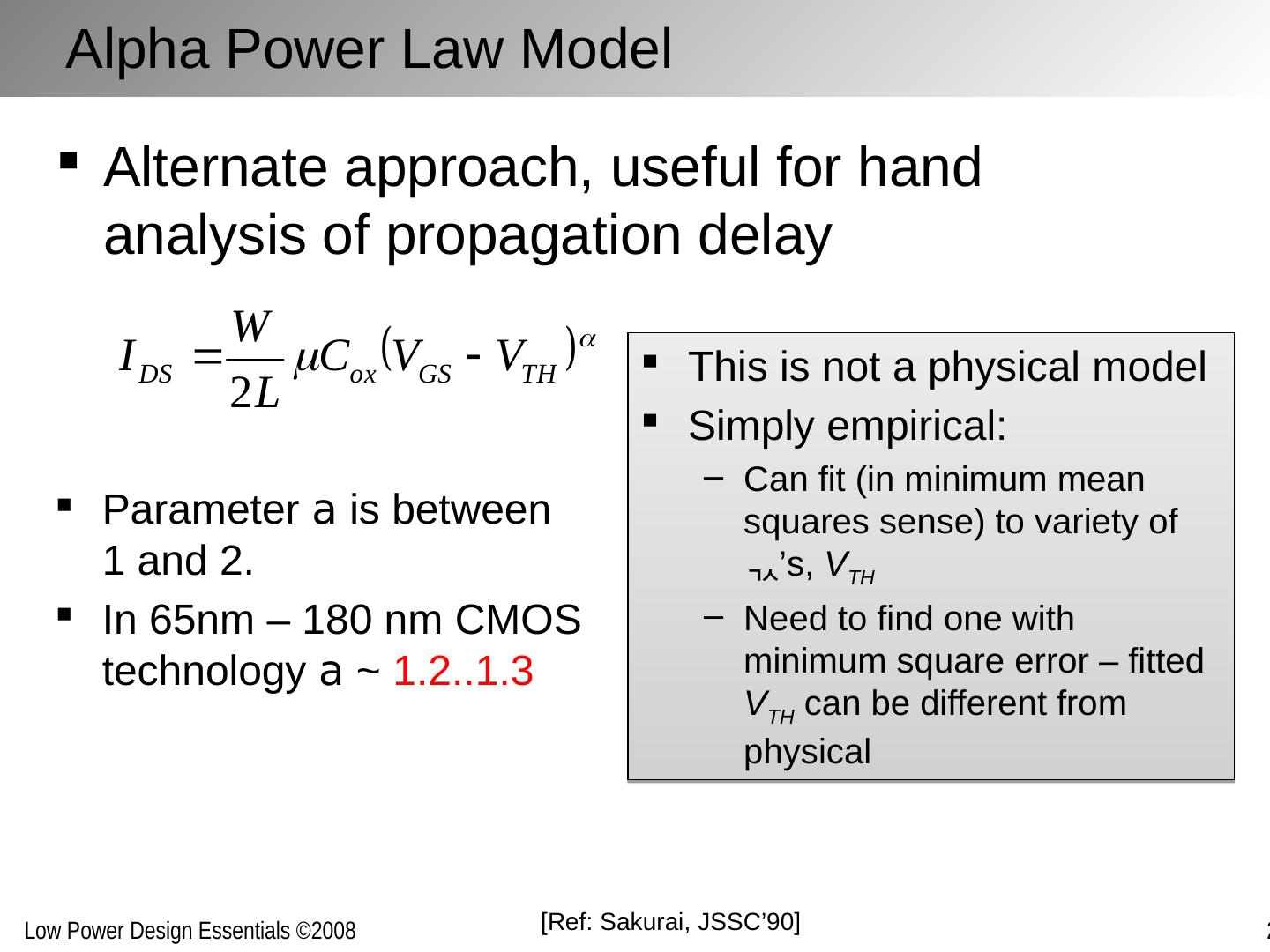
9 .Alpha Power Law Model Alternate approach, useful for hand analysis of propagation delay Parameter a is between 1 and 2. In 65nm – 180 nm CMOS technology a ~ 1.2..1.3 [Ref: Sakurai , JSSC’90 ] This is not a physical model Simply empirical: Can fit (in minimum mean squares sense) to variety of ’s, V TH Need to find one with minimum square error – fitted V TH can be different from physical
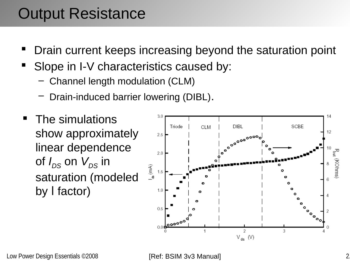
10 .Output Resistance Drain current keeps increasing beyond the saturation point Slope in I-V characteristics caused by: Channel length modulation (CLM) Drain-induced barrier lowering (DIBL) . [Ref: BSIM 3v3 Manual] The simulations show approximately linear dependence of I DS on V DS in saturation (modeled by l factor)
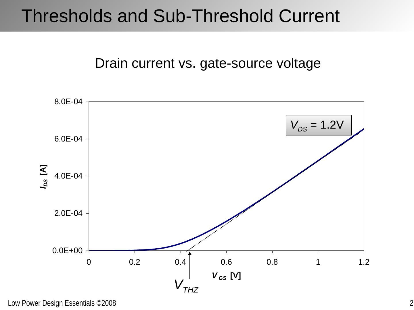
11 .Thresholds and Sub-Threshold Current Drain current vs. gate-source voltage V THZ V DS = 1.2V
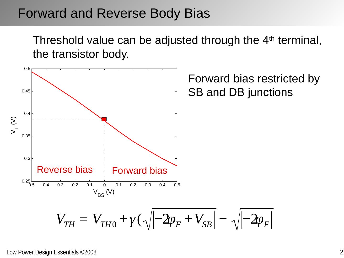
12 .Forward and Reverse Body Bias Threshold value can be adjusted through the 4 th terminal, the transistor body. Forward bias Reverse bias Forward bias restricted by SB and DB junctions
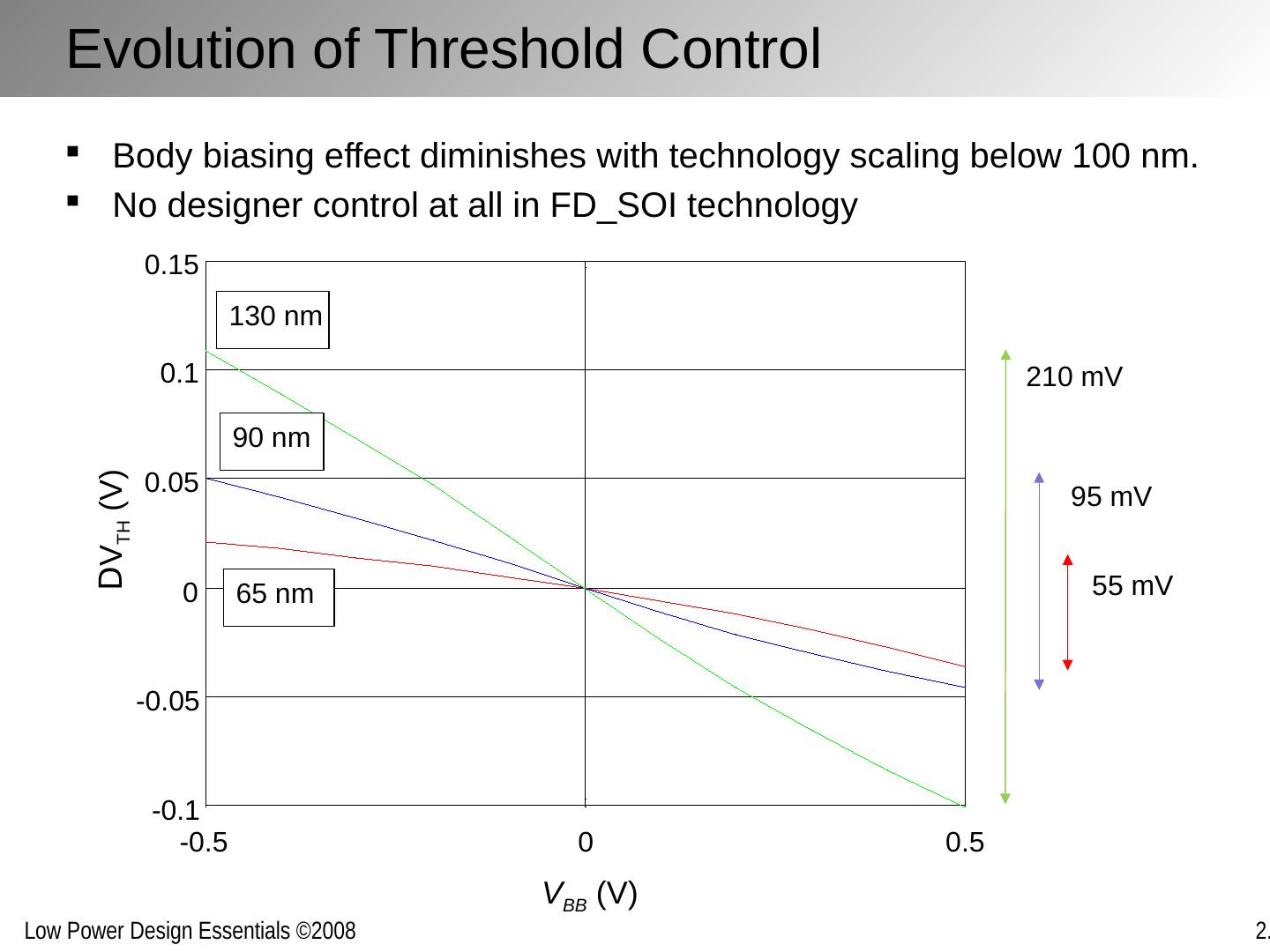
13 .Evolution of Threshold Control -0.5 0 0.5 -0.1 -0.05 0 0.05 0.1 0.15 V BB (V) D V TH (V) 130 nm 90 nm 65 nm Body biasing effect diminishes with technology scaling below 100 nm. No designer control at all in FD_SOI technology 210 mV 95 mV 55 mV
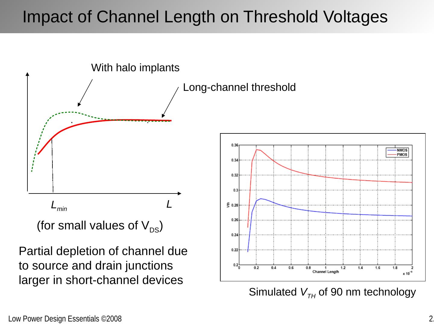
14 .Impact of Channel Length on Threshold Voltages L Long-channel threshold L min With halo implants (for small values of V DS ) Partial depletion of channel due to source and drain junctions larger in short-channel devices Simulated V TH of 90 nm technology
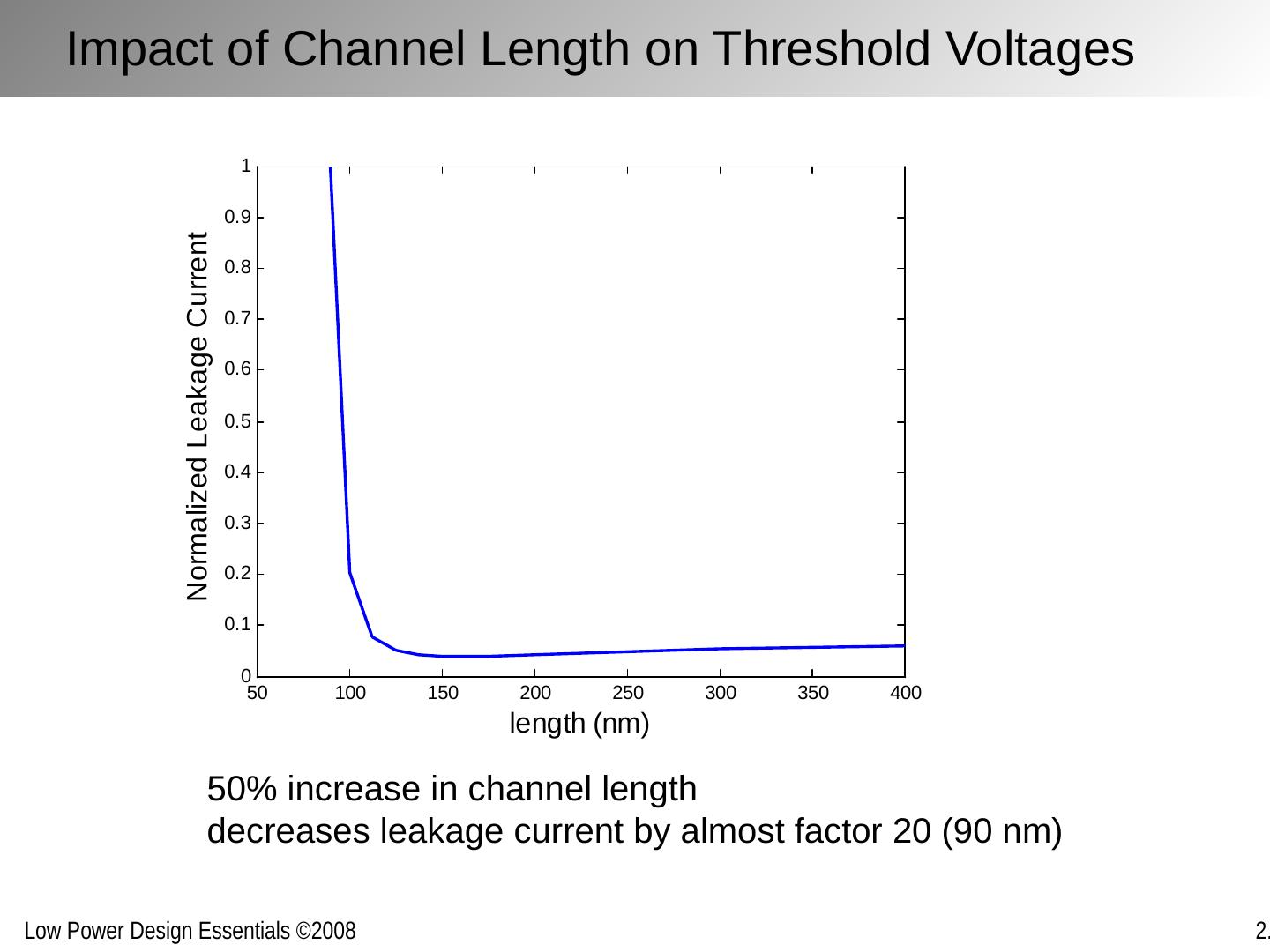
15 .Impact of Channel Length on Threshold Voltages 50% increase in channel length decreases leakage current by almost factor 20 (90 nm)
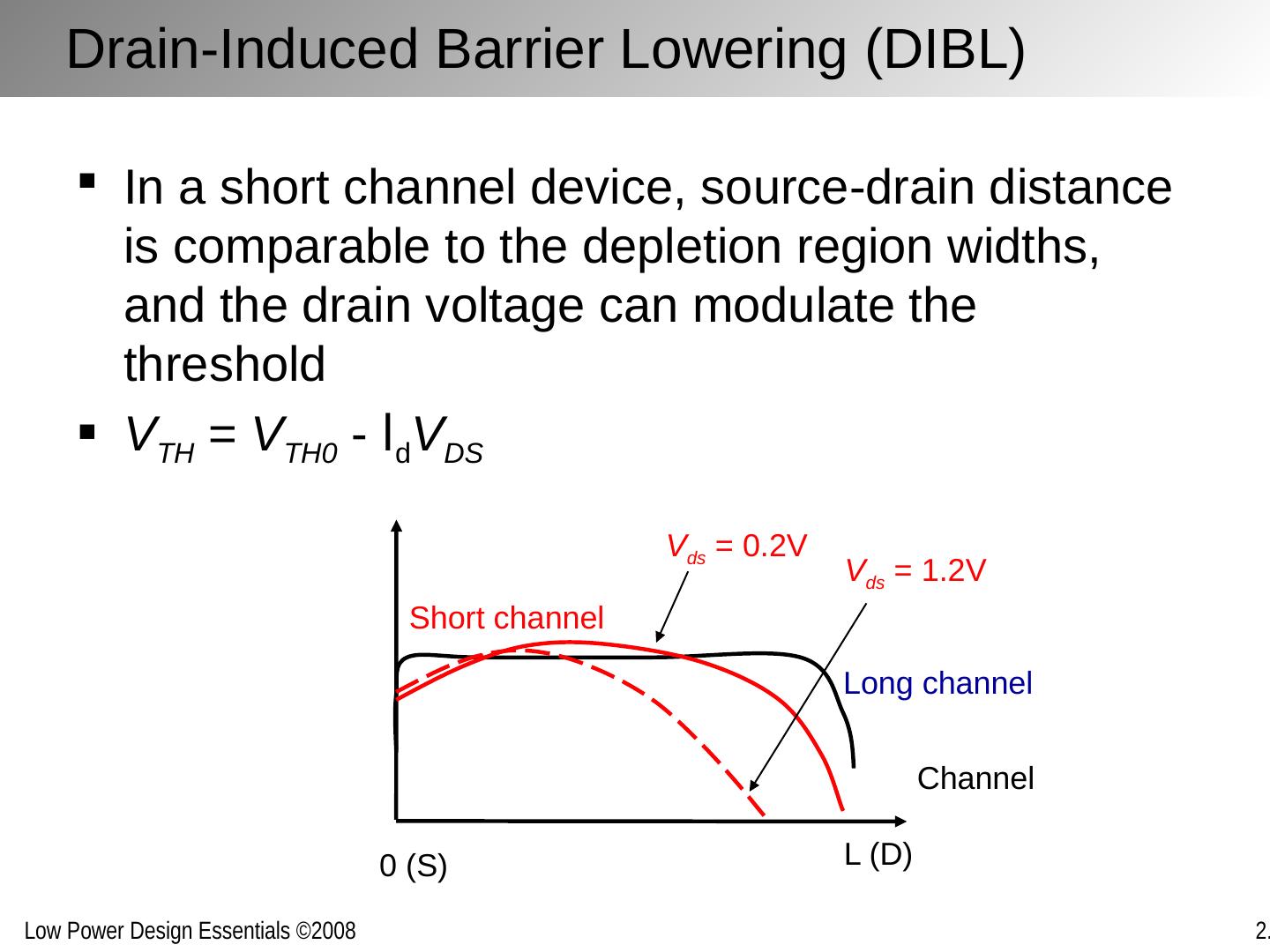
16 .Drain-Induced Barrier Lowering (DIBL) In a short channel device, source-drain distance is comparable to the depletion region widths, and the drain voltage can modulate the threshold V TH = V TH0 - l d V DS Channel L (D) 0 (S) Long channel Short channel V ds = 0.2V V ds = 1.2V
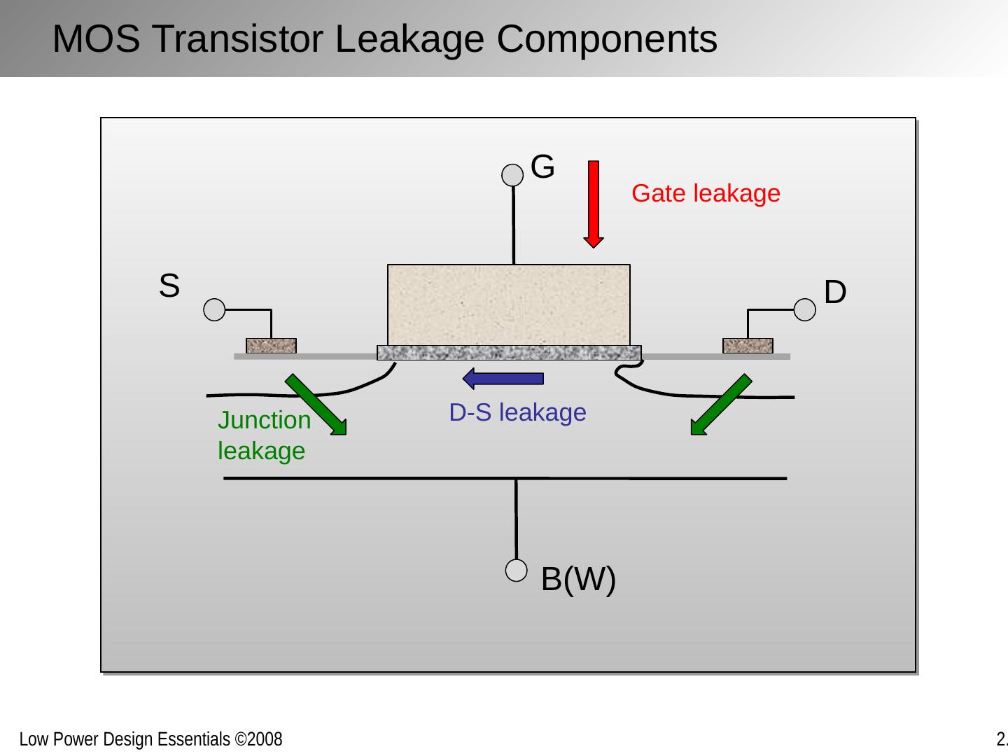
17 .MOS Transistor Leakage Components G D S B(W) Gate leakage D-S leakage Junction leakage
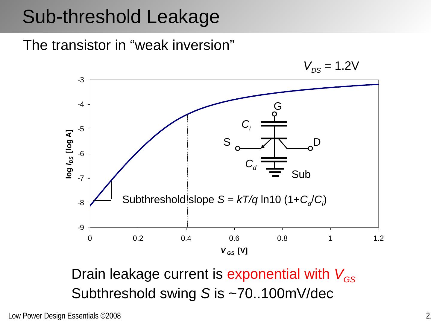
18 .Sub-threshold Leakage Subthreshold slope S = kT/q ln10 (1+ C d / C i ) Drain leakage current is exponential with V GS Subthreshold swing S is ~70..100mV/dec V DS = 1.2V G S D Sub C i C d The transistor in “weak inversion”
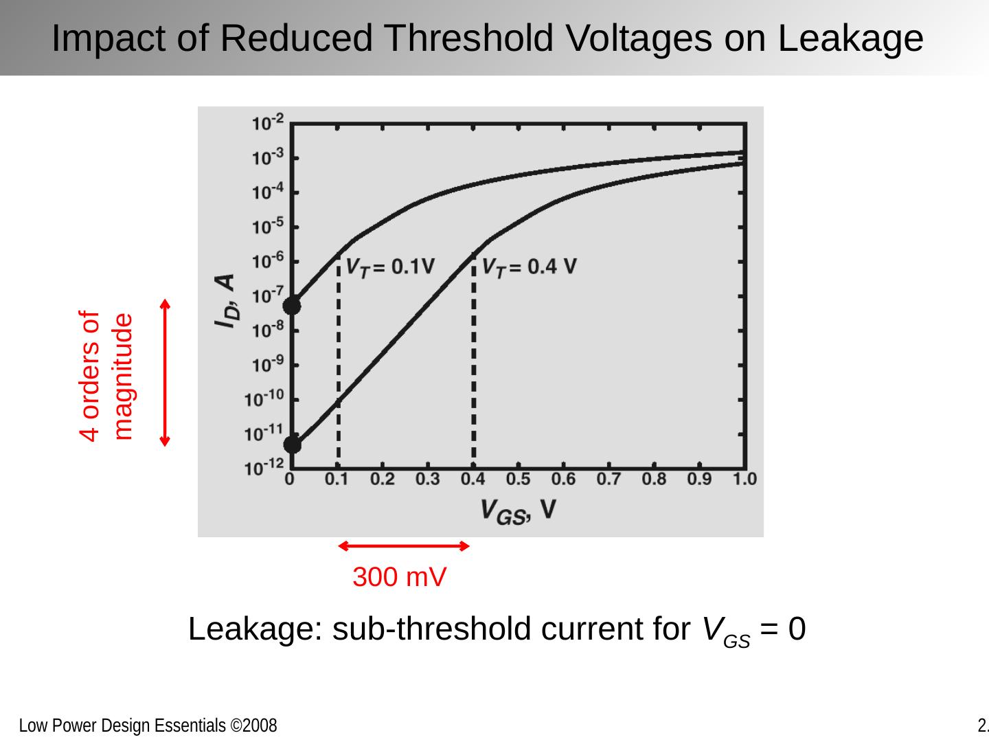
19 .Impact of Reduced Threshold Voltages on Leakage 4 orders of magnitude 300 mV Leakage: sub-threshold current for V GS = 0
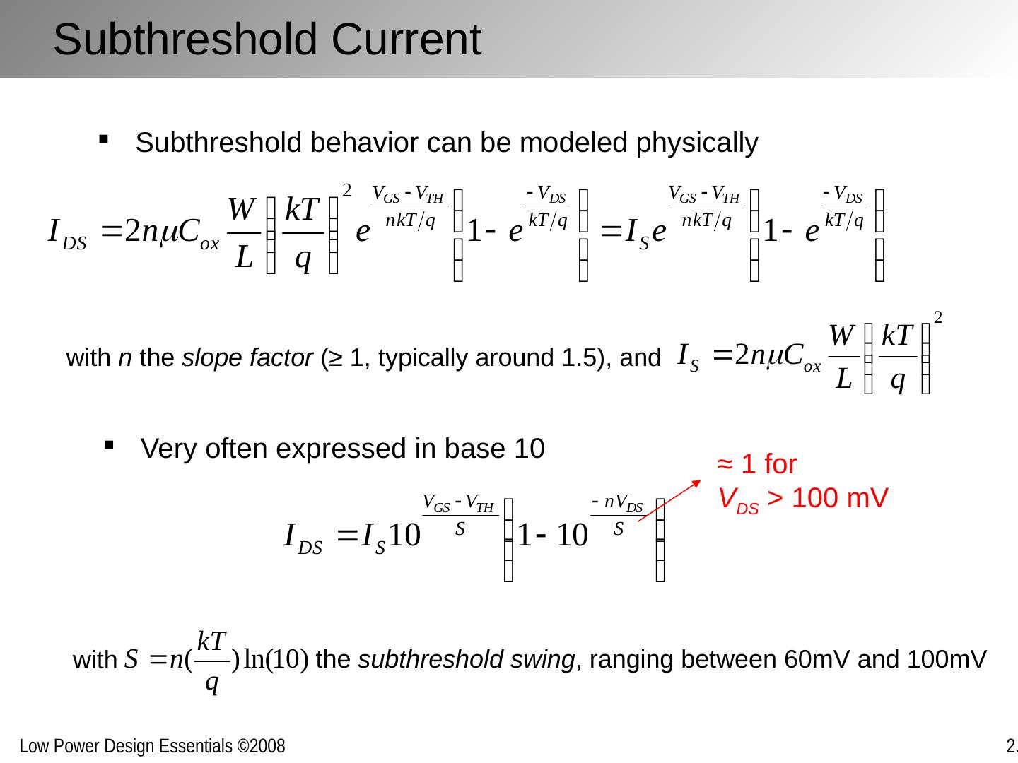
20 .Subthreshold Current Subthreshold behavior can be modeled physically with n the slope factor (≥ 1, typically around 1.5), and Very often expressed in base 10 the subthreshold swing , ranging between 60mV and 100mV with ≈ 1 for V DS > 100 mV
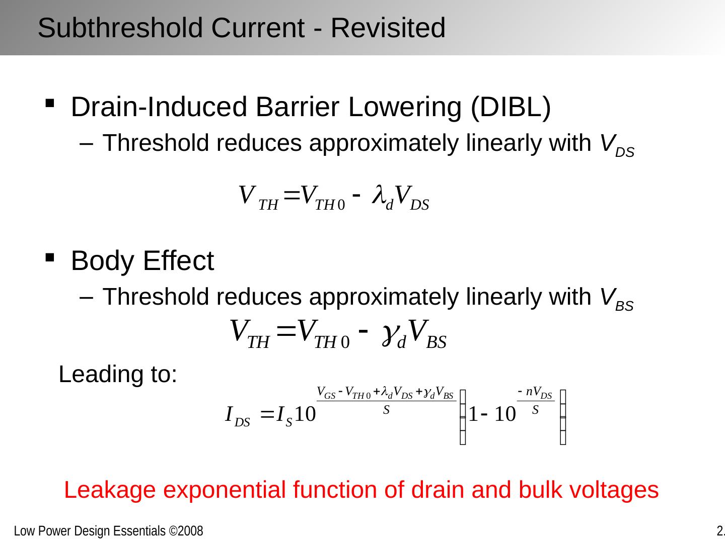
21 .Subthreshold Current - Revisited Drain-Induced Barrier Lowering (DIBL) Threshold reduces approximately linearly with V DS Body Effect Threshold reduces approximately linearly with V BS Leading to: Leakage exponential function of drain and bulk voltages
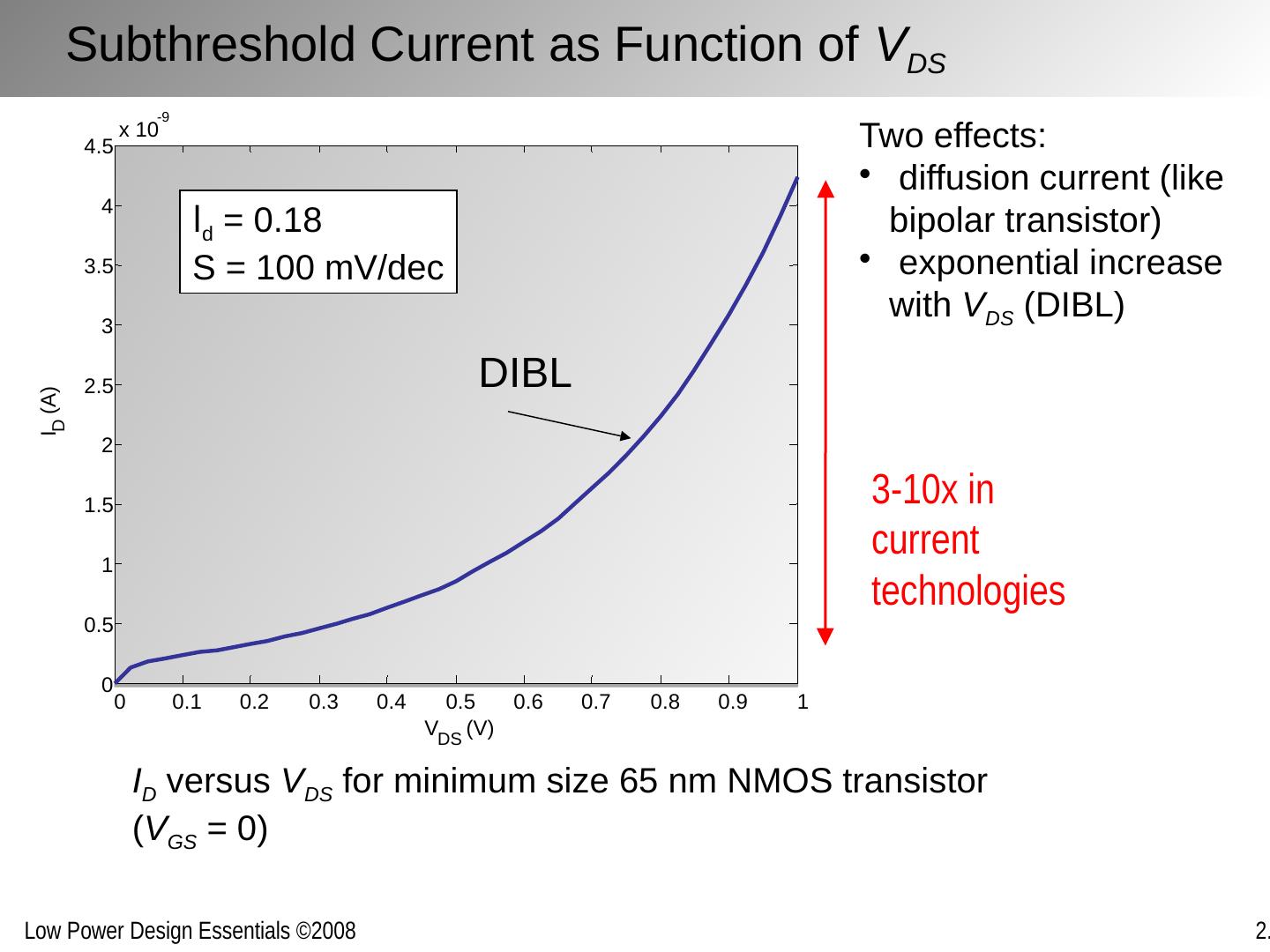
22 .Subthreshold Current as Function of V DS I D versus V DS for minimum size 65 nm NMOS transistor ( V GS = 0) l d = 0.18 S = 100 mV/dec DIBL 0 0.1 0.2 0.3 0.4 0.5 0.6 0.7 0.8 0.9 1 0 0.5 1 1.5 2 2.5 3 3.5 4 4.5 x 10 -9 V DS (V) I D (A) Two effects: diffusion current (like bipolar transistor) exponential increase with V DS (DIBL) 3-10x in current technologies
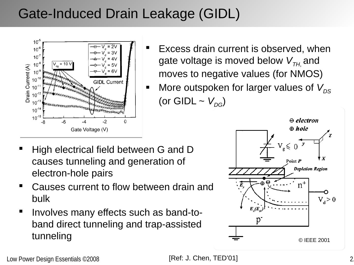
23 .Gate-Induced Drain Leakage (GIDL) Excess drain current is observed, when gate voltage is moved below V TH , and moves to negative values (for NMOS) More outspoken for larger values of V DS (or GIDL ~ V DG ) High electrical field between G and D causes tunneling and generation of electron-hole pairs Causes current to flow between drain and bulk Involves many effects such as band-to-band direct tunneling and trap-assisted tunneling [Ref: J. Chen, TED’01] © IEEE 2001
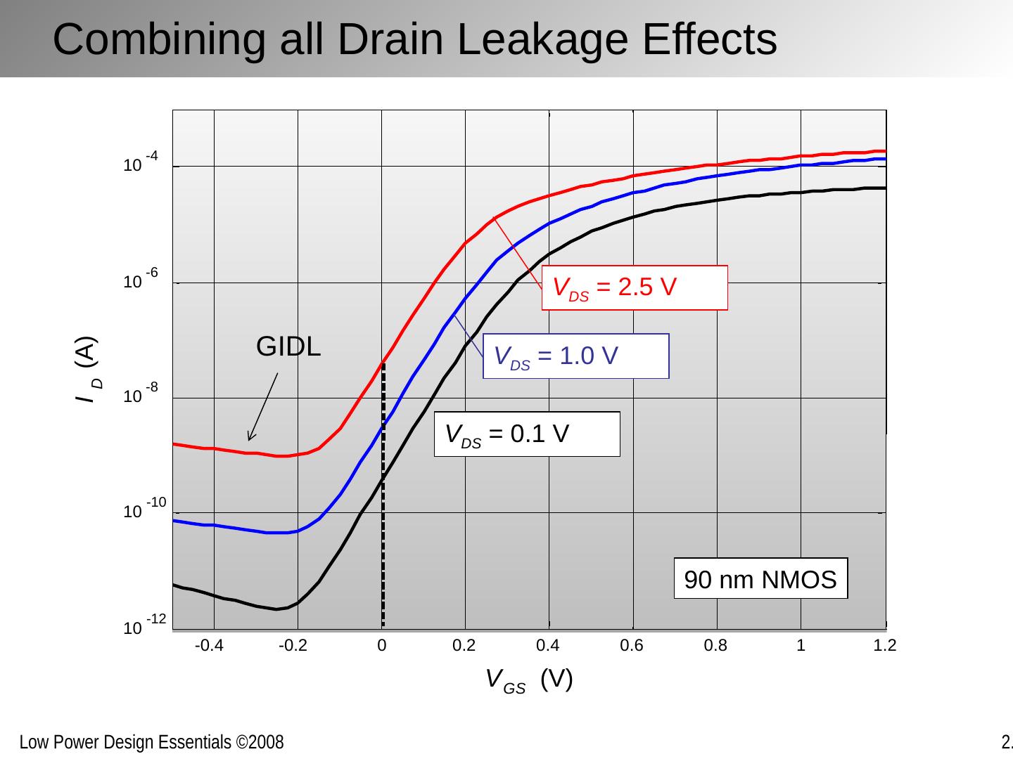
24 .Combining all Drain Leakage Effects -0.4 -0.2 0 0.2 0.4 0.6 0.8 1 1.2 10 -12 10 -10 10 -8 10 -6 10 -4 V GS (V) I D (A) V DS = 0.1 V V DS = 1.0 V V DS = 2.5 V 90 nm NMOS GIDL
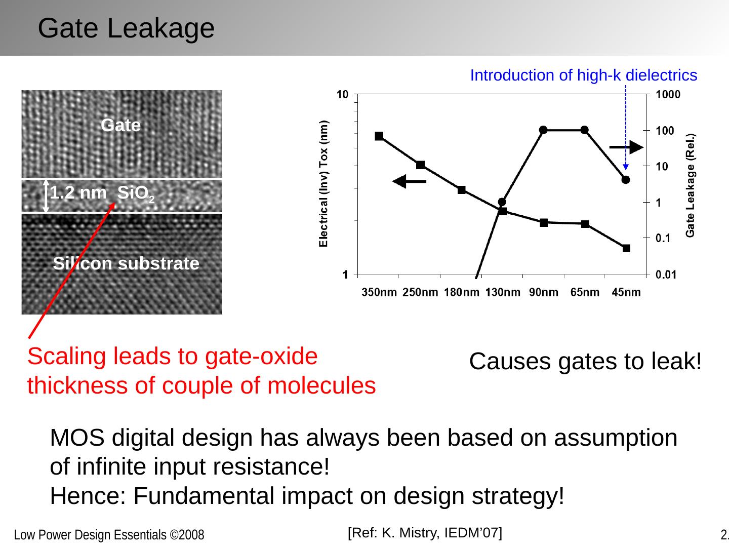
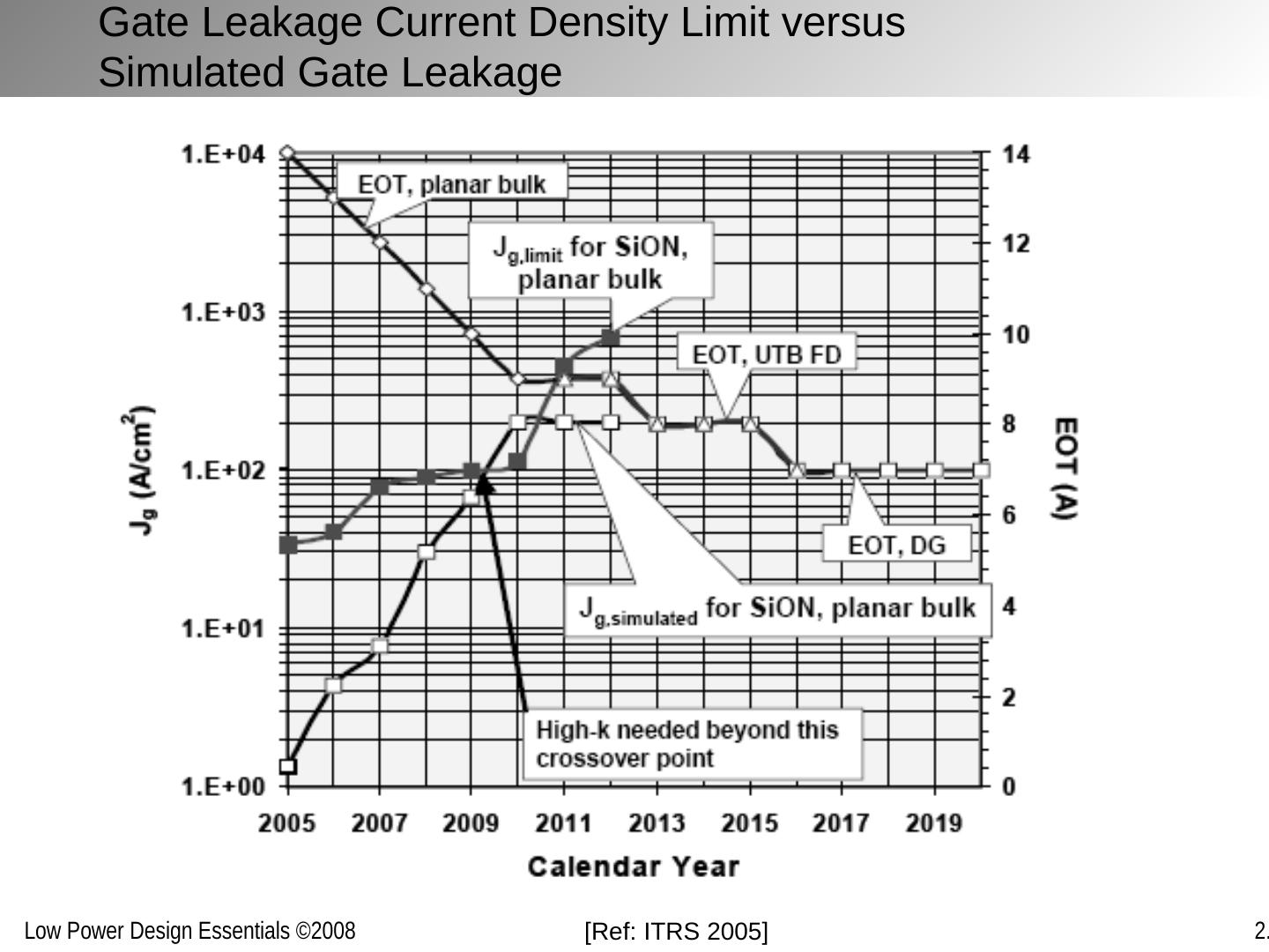
25 .Gate Leakage Silicon substrate 1.2 nm SiO 2 Gate Scaling leads to gate-oxide thickness of couple of molecules MOS digital design has always been based on assumption of infinite input resistance! Hence: Fundamental impact on design strategy! Causes gates to leak! [Ref: K. Mistry , IEDM’07] Introduction of high- k dielectrics
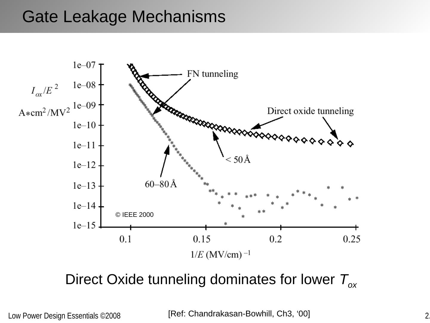
26 .Gate Leakage Mechanisms Direct Oxide tunneling dominates for lower T ox [Ref: Chandrakasan-Bowhill , Ch3, ‘00 ] © IEEE 2000
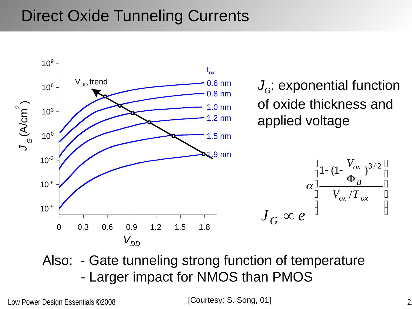
27 .Direct Oxide Tunneling Currents V DD J G (A/cm 2 ) 0 0.3 0.6 0.9 1.2 1.5 1.8 10 -9 10 -6 10 -3 10 0 10 3 10 6 10 9 t ox 0.6 nm 0.8 nm 1.0 nm 1.2 nm 1.5 nm 1.9 nm V DD trend [Courtesy: S. Song, 01] Also: - Gate tunneling strong function of temperature - Larger impact for NMOS than PMOS J G : exponential function of oxide thickness and applied voltage
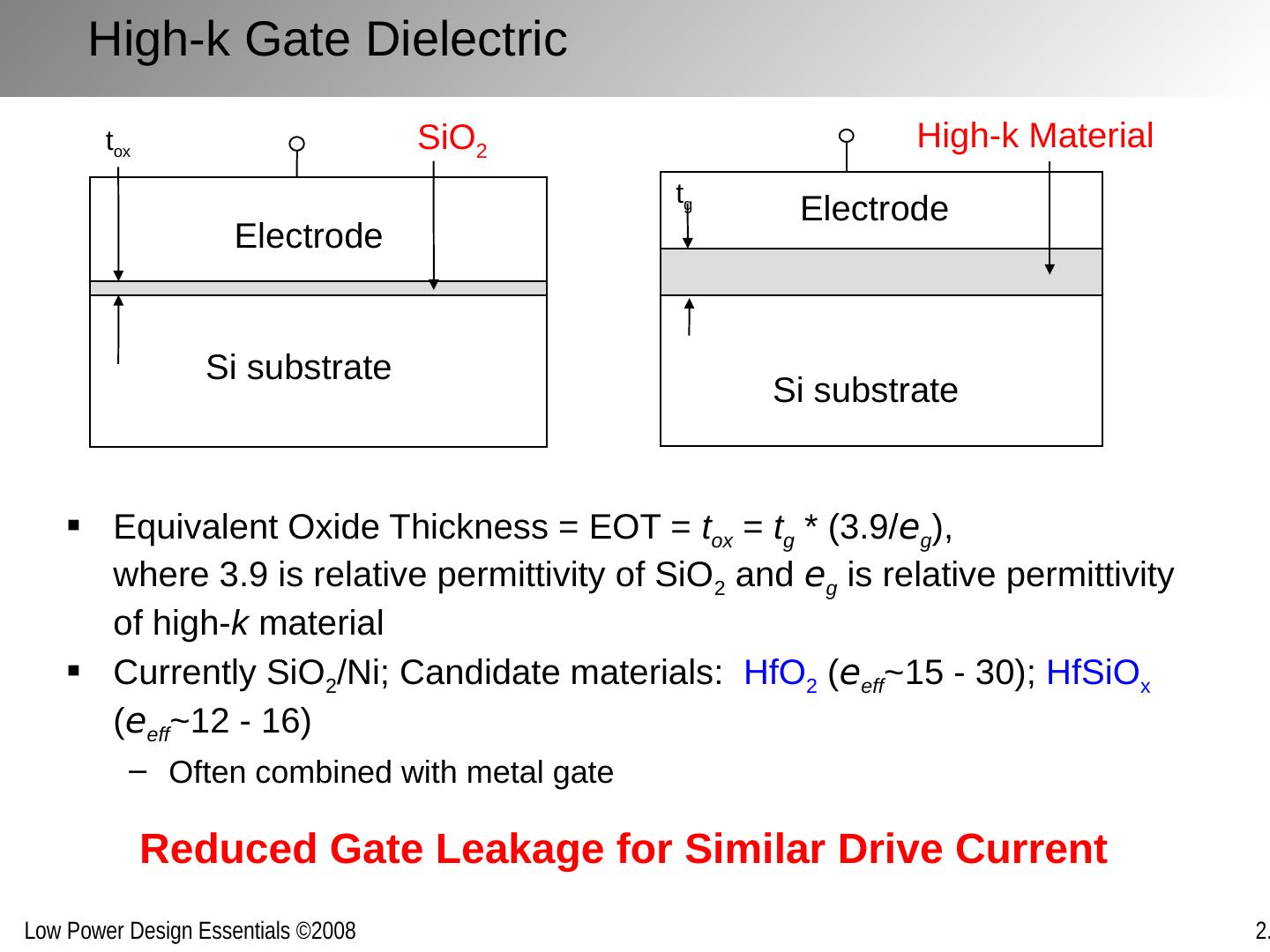
28 .High-k Gate Dielectric Equivalent Oxide Thickness = EOT = t ox = t g * (3.9/ e g ), where 3.9 is relative permittivity of SiO 2 and e g is relative permittivity of high- k material Currently SiO 2 /Ni; Candidate materials: HfO 2 ( e eff ~15 - 30); HfSiO x ( e eff ~12 - 16) Often combined with metal gate Electrode Si substrate t ox SiO 2 t g High-k Material Electrode Si substrate Reduced Gate Leakage for Similar Drive Current
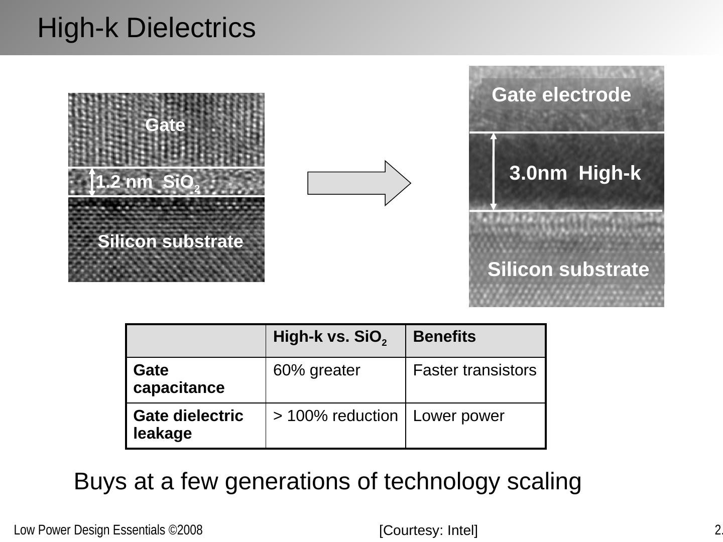
29 .High-k Dielectrics Silicon substrate 1.2 nm SiO 2 Gate Silicon substrate Gate electrode 3.0nm High-k Buys at a few generations of technology scaling [Courtesy: Intel] High-k vs. SiO 2 Benefits Gate capacitance 60% greater Faster transistors Gate dielectric leakage > 100% reduction Lower power


