- 快召唤伙伴们来围观吧
- 微博 QQ QQ空间 贴吧
- 文档嵌入链接
- 复制
- 微信扫一扫分享
- 已成功复制到剪贴板
金属半导体接触,泊松方程,功函数,M-S能带图
展开查看详情
1 . Lecture #8 OUTLINE • Poisson’s Equation • Work Function • Metal-Semiconductor Contacts – equilibrium energy-band diagram – depletion-layer width Reading: Chapter 5.1.2,14.1, 14.2 Spring 2003 EE130 Lecture 8, Slide 1 Poisson’s Equation Gauss’s Law: area A εs : permittivity (F/cm) (x) (x+∆x) ρ : charge density (C/cm3) ∆x Spring 2003 EE130 Lecture 8, Slide 2 1
2 . Charge Density in a Semiconductor • Assuming the dopants are completely ionized: ρ = q (p – n + ND – NA) Spring 2003 EE130 Lecture 8, Slide 3 Work Function Ε0: vacuum energy level ΦM: metal work function ΦS: semiconductor work function Spring 2003 EE130 Lecture 8, Slide 4 2
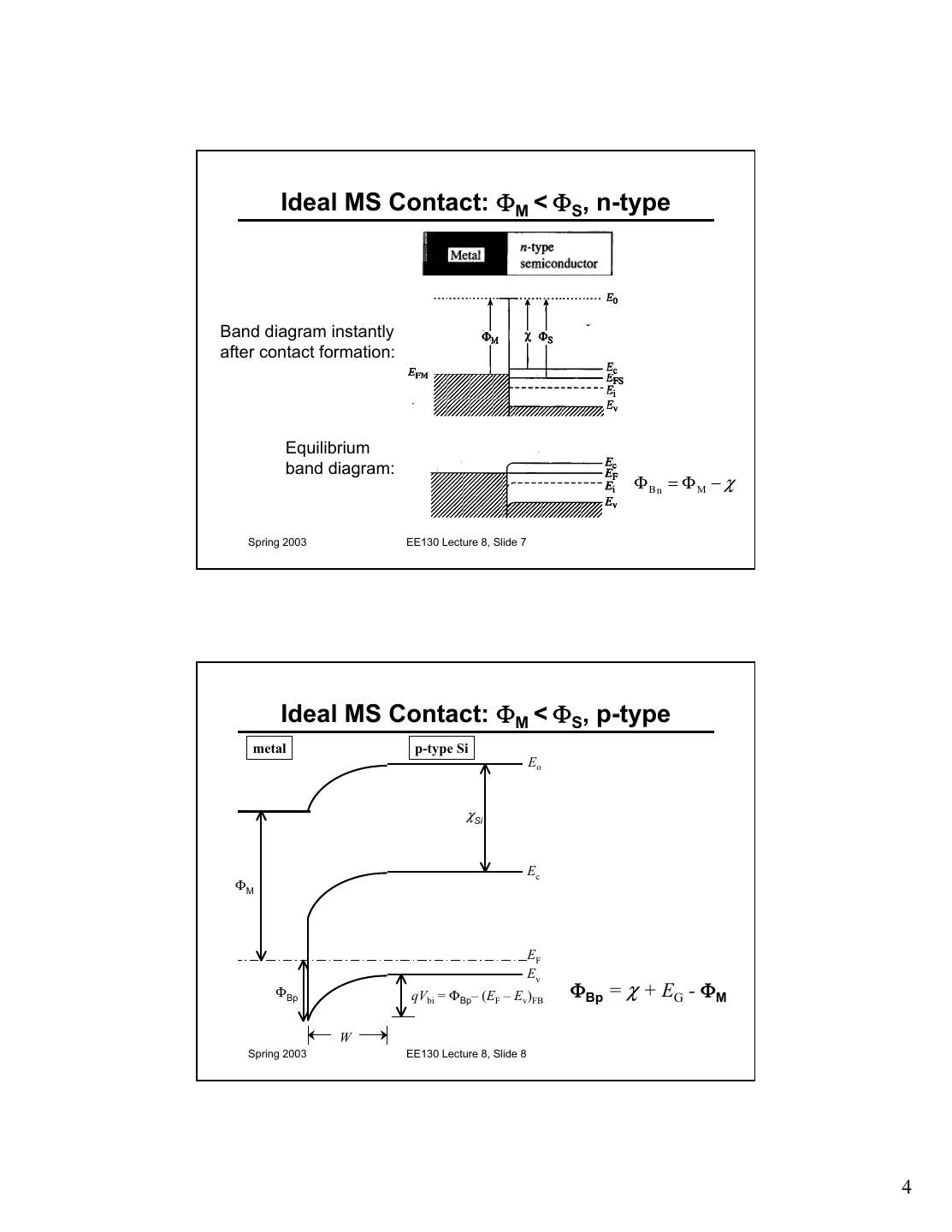
3 . Metal-Semiconductor Contacts There are 2 kinds of metal-semiconductor contacts: • rectifying “Schottky diode” • non-rectifying “ohmic contact” Spring 2003 EE130 Lecture 8, Slide 5 Ideal MS Contact: ΦM > ΦS, n-type Band diagram instantly after contact formation: Schottky Equilibrium Barrier : band diagram: Φ Bn = Φ M − χ Spring 2003 EE130 Lecture 8, Slide 6 3
4 . Ideal MS Contact: ΦM < ΦS, n-type Band diagram instantly after contact formation: Equilibrium band diagram: Φ Bn = Φ M − χ Spring 2003 EE130 Lecture 8, Slide 7 Ideal MS Contact: ΦM < ΦS, p-type metal p-type Si Eo χSi Ec ΦM EF Ev ΦBp qVbi = ΦBp– (EF – Ev)FB ΦBp = χ + EG - ΦM W Spring 2003 EE130 Lecture 8, Slide 8 4
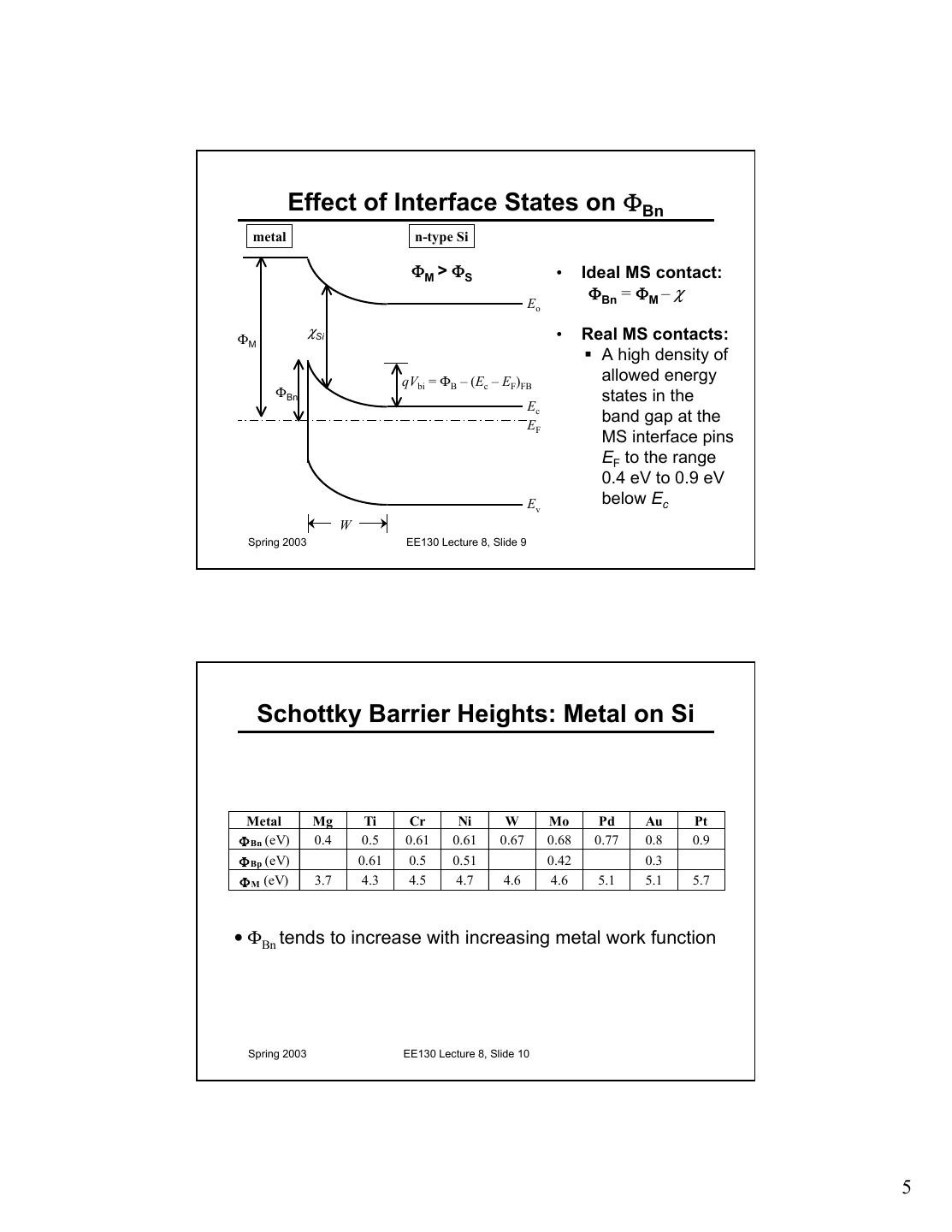
5 . Effect of Interface States on ΦBn metal n-type Si ΦM > ΦS • Ideal MS contact: ΦBn = ΦM – χ Eo χSi • Real MS contacts: ΦM A high density of qVbi = ΦB – (Ec – EF)FB allowed energy ΦBn states in the Ec EF band gap at the MS interface pins EF to the range 0.4 eV to 0.9 eV Ev below Ec W Spring 2003 EE130 Lecture 8, Slide 9 Schottky Barrier Heights: Metal on Si Metal Mg Ti Cr Ni W Mo Pd Au Pt Φ Bn (eV) 0.4 0.5 0.61 0.61 0.67 0.68 0.77 0.8 0.9 Φ Bp (eV) 0.61 0.5 0.51 0.42 0.3 Φ M (eV) 3.7 4.3 4.5 4.7 4.6 4.6 5.1 5.1 5.7 • ΦBn tends to increase with increasing metal work function Spring 2003 EE130 Lecture 8, Slide 10 5
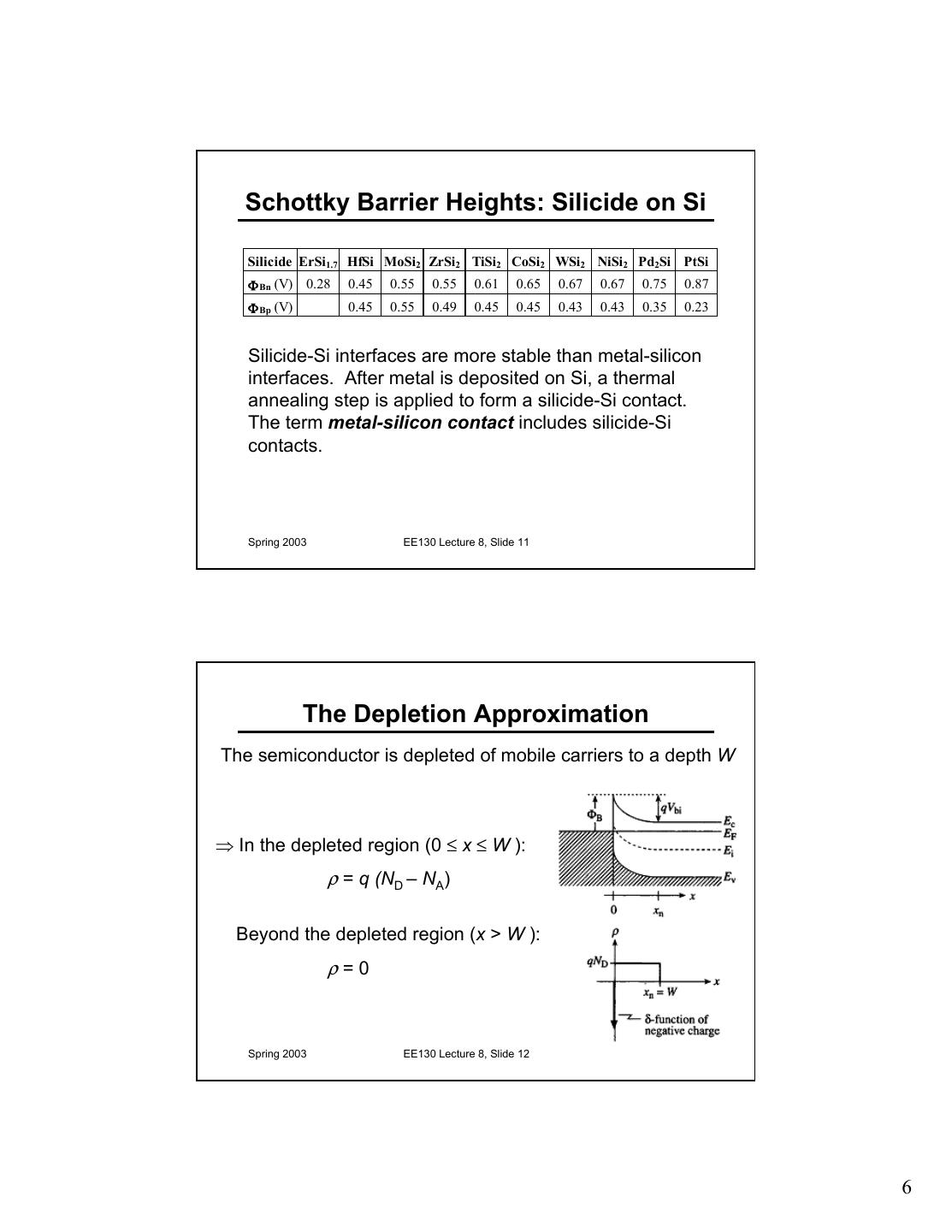
6 . Schottky Barrier Heights: Silicide on Si Silicide ErSi1.7 HfSi MoSi2 ZrSi2 TiSi2 CoSi2 WSi2 NiSi2 Pd2Si PtSi Φ Bn (V) 0.28 0.45 0.55 0.55 0.61 0.65 0.67 0.67 0.75 0.87 Φ Bp (V) 0.45 0.55 0.49 0.45 0.45 0.43 0.43 0.35 0.23 Silicide-Si interfaces are more stable than metal-silicon interfaces. After metal is deposited on Si, a thermal annealing step is applied to form a silicide-Si contact. The term metal-silicon contact includes silicide-Si contacts. Spring 2003 EE130 Lecture 8, Slide 11 The Depletion Approximation The semiconductor is depleted of mobile carriers to a depth W ⇒ In the depleted region (0 ≤ x ≤ W ): ρ = q (ND – NA) Beyond the depleted region (x > W ): ρ=0 Spring 2003 EE130 Lecture 8, Slide 12 6
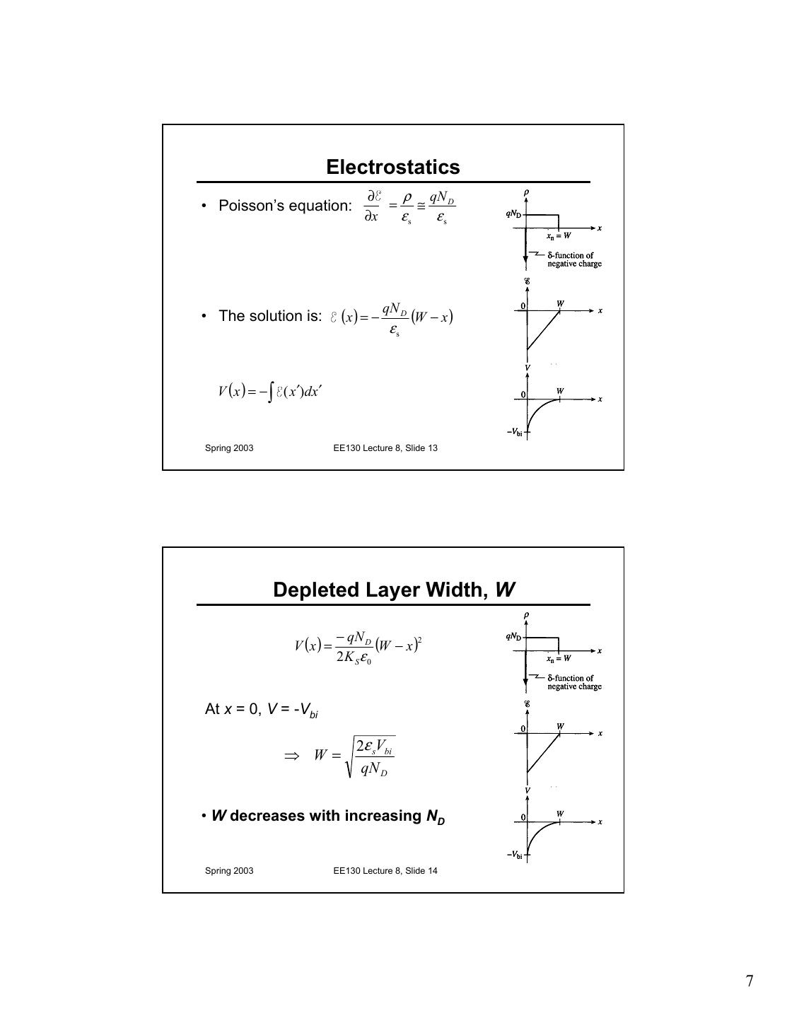
7 . Electrostatics ∂ ρ qN D • Poisson’s equation: = ≅ ∂x εs εs • The solution is: (x ) = − qN D (W − x ) εs V ( x ) = − ∫ ( x′)dx′ Spring 2003 EE130 Lecture 8, Slide 13 Depleted Layer Width, W − qN D V (x ) = (W − x )2 2K Sε 0 At x = 0, V = -Vbi 2ε sVbi ⇒ W= qN D • W decreases with increasing ND Spring 2003 EE130 Lecture 8, Slide 14 7
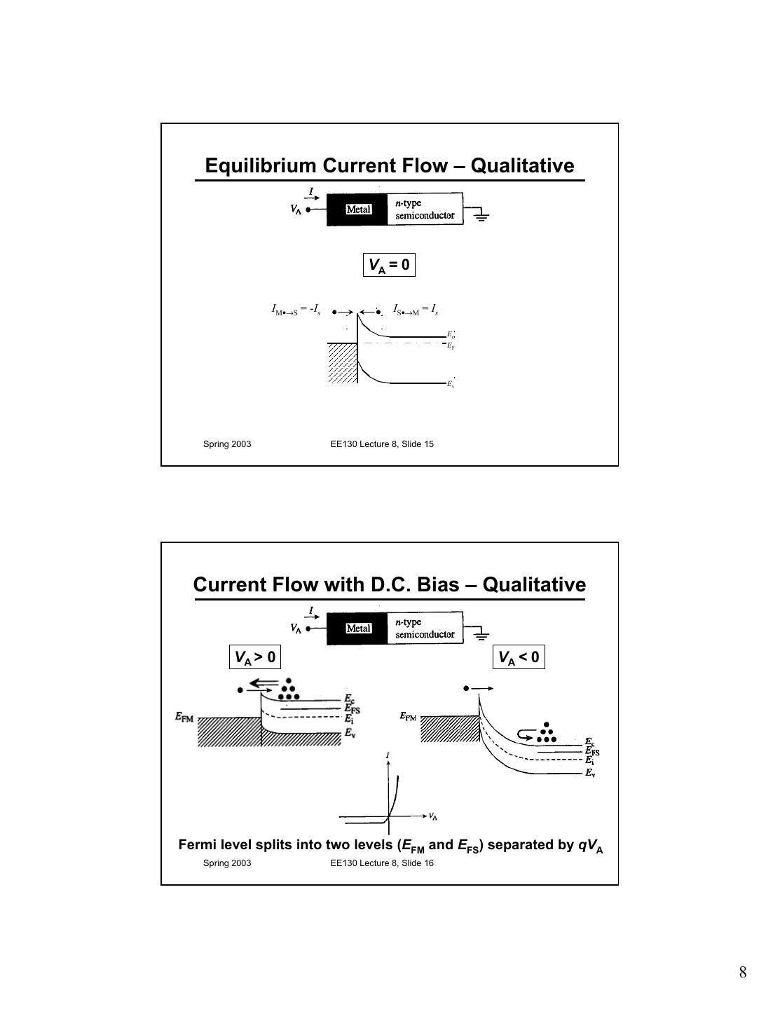
8 . Equilibrium Current Flow – Qualitative VA = 0 IM•→S = -Is IS•→M = Is Ec EF Ev Spring 2003 EE130 Lecture 8, Slide 15 Current Flow with D.C. Bias – Qualitative VA > 0 VA < 0 Fermi level splits into two levels (EFM and EFS) separated by qVA Spring 2003 EE130 Lecture 8, Slide 16 8
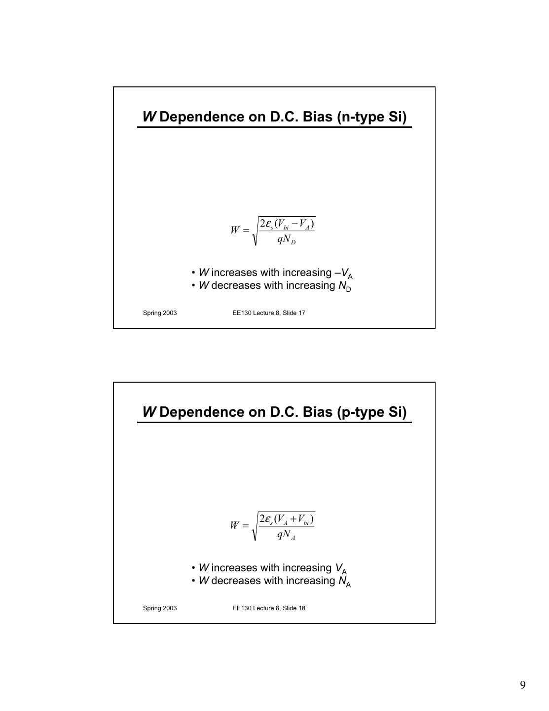
9 .W Dependence on D.C. Bias (n-type Si) 2ε s (Vbi − VA ) W= qN D • W increases with increasing –VA • W decreases with increasing ND Spring 2003 EE130 Lecture 8, Slide 17 W Dependence on D.C. Bias (p-type Si) 2ε s (VA + Vbi ) W= qN A • W increases with increasing VA • W decreases with increasing NA Spring 2003 EE130 Lecture 8, Slide 18 9


