- 快召唤伙伴们来围观吧
- 微博 QQ QQ空间 贴吧
- 文档嵌入链接
- 复制
- 微信扫一扫分享
- 已成功复制到剪贴板
小信号模型与瞬态响应
展开查看详情
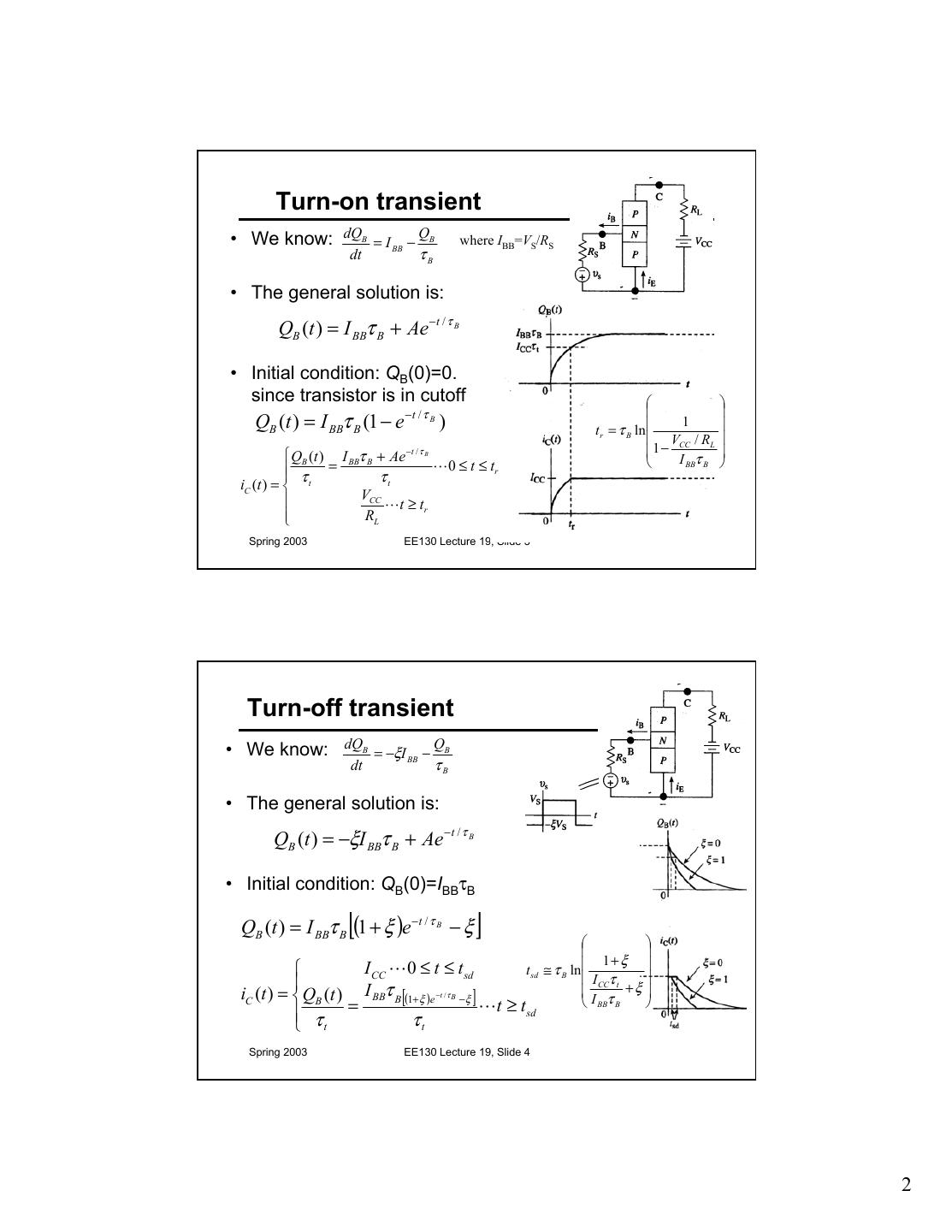
1 . Lecture #19 ANNOUNCEMENT • Quiz #4 (Thursday 4/3) to cover Chapters 10 & 11 OUTLINE • BJT transient response • BJT small-signal model, fT Reading: Chapter 12 Spring 2003 EE130 Lecture 19, Slide 1 BJT Switching - Qualitative Spring 2003 EE130 Lecture 19, Slide 2 1
2 . Turn-on transient • We know: dQB = I BB − QB where IBB=VS/RS dt τB • The general solution is: QB (t ) = I BBτ B + Ae − t / τ B • Initial condition: QB(0)=0. since transistor is in cutoff QB (t ) = I BBτ B (1 − e − t / τ B ) t r = τ B ln 1 VCC / RL QB (t ) I BBτ B + Ae − t / τ B 1− I τ τ = τt L0 ≤ t ≤ tr BB B iC (t ) = t VCC Lt ≥ t r RL Spring 2003 EE130 Lecture 19, Slide 3 Turn-off transient • We know: dQB = −ξI BB − QB dt τB • The general solution is: QB (t ) = −ξI BBτ B + Ae − t / τ B • Initial condition: QB(0)=IBBτB [ QB (t ) = I BBτ B (1 + ξ )e − t / τ B − ξ ] 1+ ξ I CC L0 ≤ t ≤ t sd t sd ≅ τ B ln I CCτ t iC (t ) = QB (t ) I BBτ B [(1+ξ )e −t / τ B −ξ ] I τ +ξ τ = Lt ≥t BB B t τt sd Spring 2003 EE130 Lecture 19, Slide 4 2
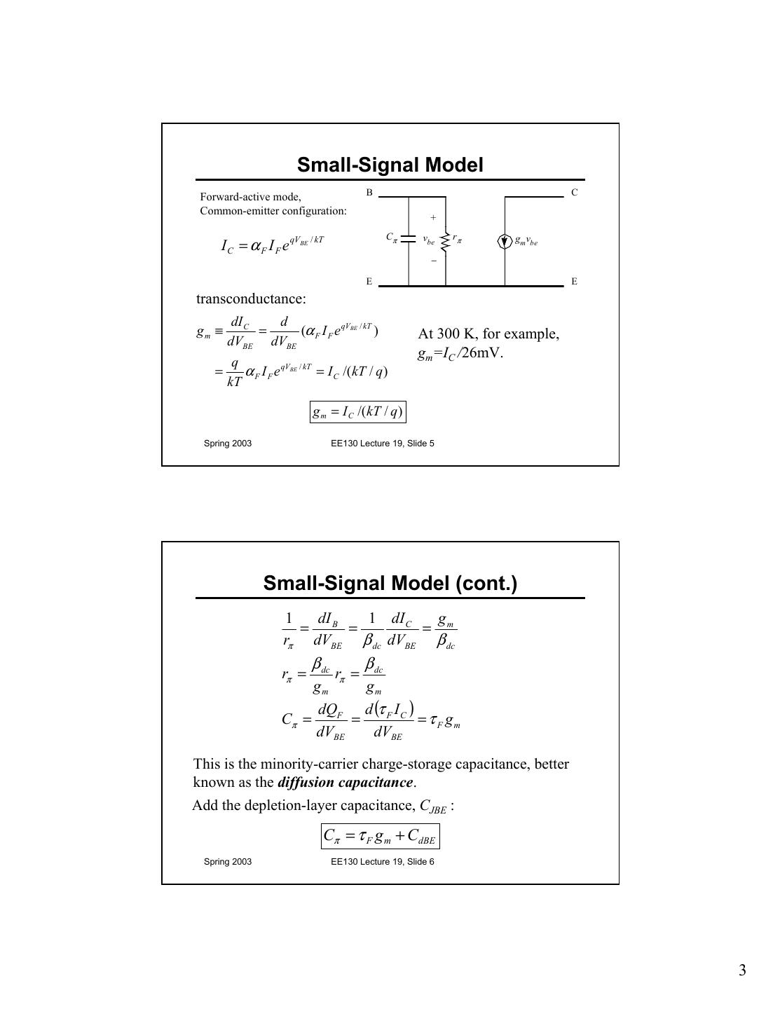
3 . Small-Signal Model B C Forward-active mode, Common-emitter configuration: + Cπ vbe rπ gm vbe I C = α F I F e qVBE / kT − E E transconductance: dI C d gm ≡ = (α F I F e qVBE / kT ) At 300 K, for example, dVBE dVBE gm=IC /26mV. q = α F I F e qVBE / kT = I C /(kT / q ) kT g m = I C /(kT / q ) Spring 2003 EE130 Lecture 19, Slide 5 Small-Signal Model (cont.) 1 dI B 1 dI C g = = = m rπ dVBE β dc dVBE β dc β dc β dc rπ = rπ = gm gm dQF d (τ F I C ) Cπ = = = τ F gm dVBE dVBE This is the minority-carrier charge-storage capacitance, better known as the diffusion capacitance. Add the depletion-layer capacitance, CJBE : Cπ = τ F g m + CdBE Spring 2003 EE130 Lecture 19, Slide 6 3
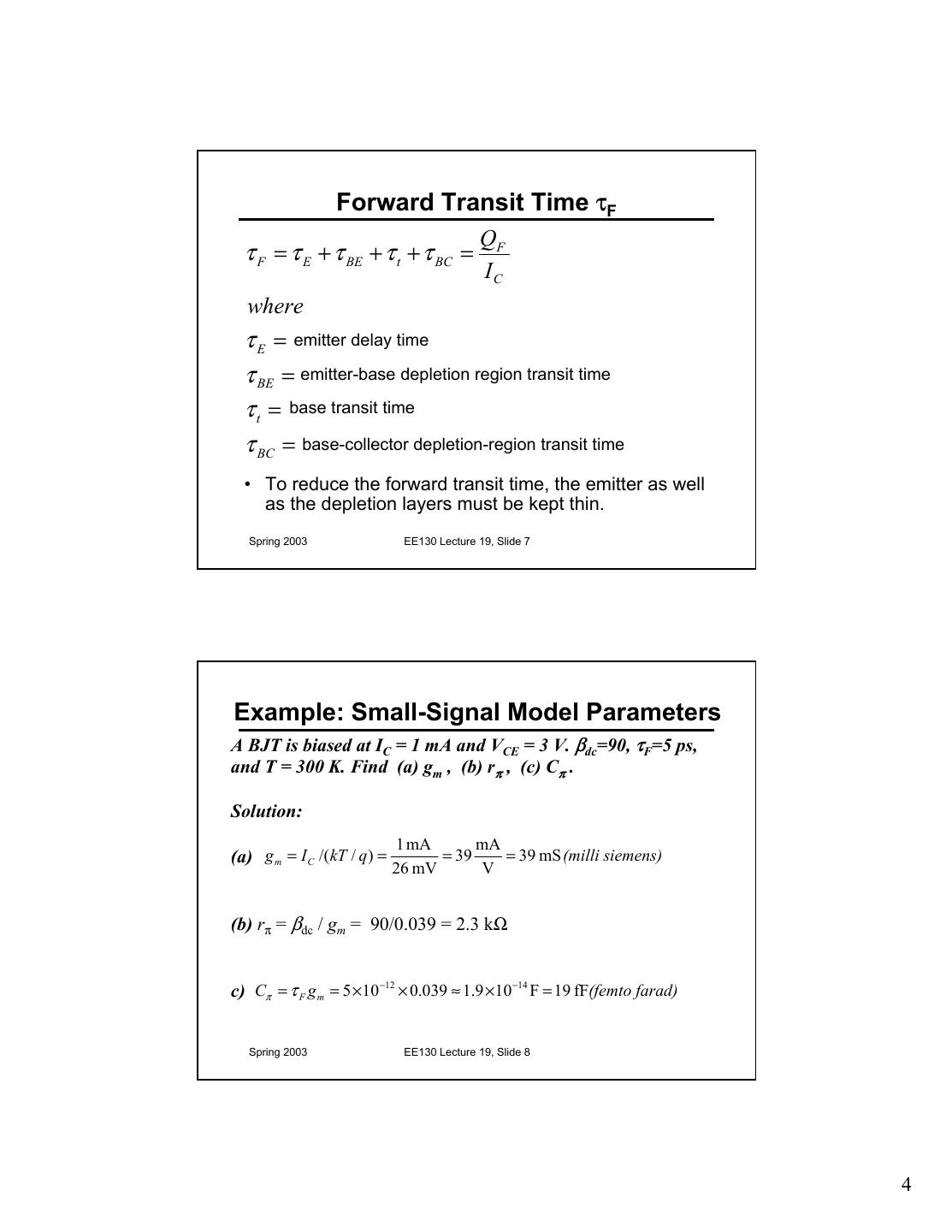
4 . Forward Transit Time τF QF τ F = τ E + τ BE + τ t + τ BC = IC where τ E = emitter delay time τ BE = emitter-base depletion region transit time τ t = base transit time τ BC = base-collector depletion-region transit time • To reduce the forward transit time, the emitter as well as the depletion layers must be kept thin. Spring 2003 EE130 Lecture 19, Slide 7 Example: Small-Signal Model Parameters A BJT is biased at IC = 1 mA and VCE = 3 V. βdc=90, τF=5 ps, and T = 300 K. Find (a) gm , (b) rπ , (c) Cπ . Solution: 1 mA mA (a) g m = I C /(kT / q) = = 39 = 39 mS (milli siemens) 26 mV V (b) rπ = βdc / gm = 90/0.039 = 2.3 kΩ c) Cπ = τ F g m = 5 ×10 −12 × 0.039 ≈ 1.9 ×10 −14 F = 19 fF(femto farad) Spring 2003 EE130 Lecture 19, Slide 8 4
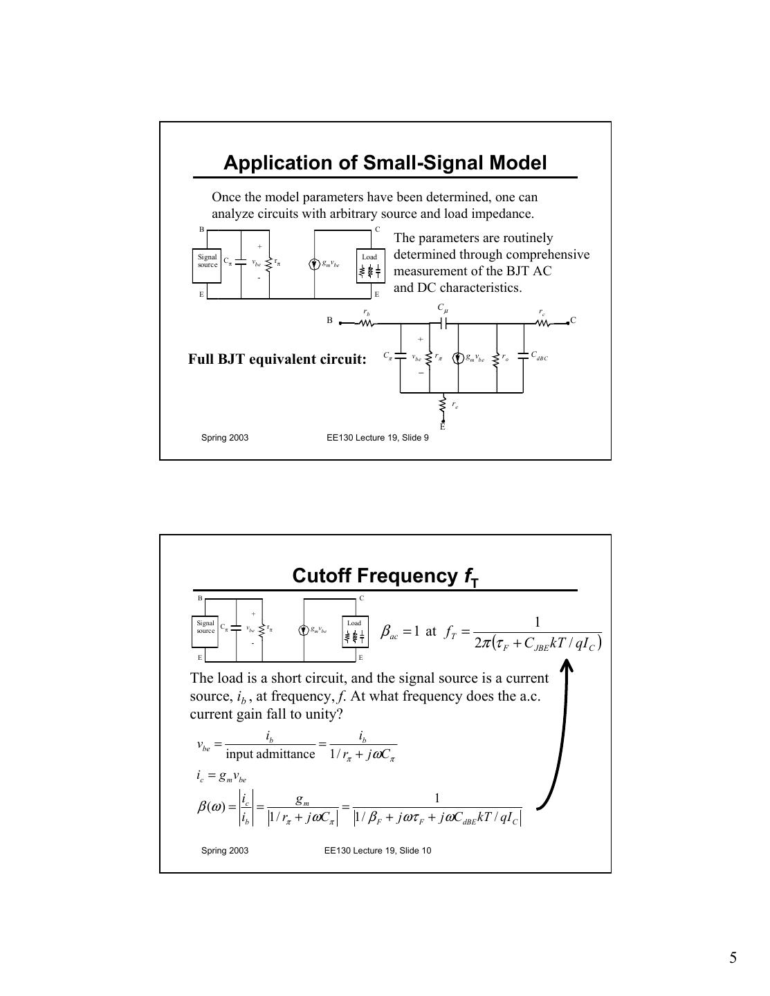
5 . Application of Small-Signal Model Once the model parameters have been determined, one can analyze circuits with arbitrary source and load impedance. B C The parameters are routinely + Signal C vbe rπ gm vbe Load determined through comprehensive source π - measurement of the BJT AC E E and DC characteristics. rb Cµ rc B C + Cπ rπ C dBC Full BJT equivalent circuit: vbe gm vbe ro − re E Spring 2003 EE130 Lecture 19, Slide 9 Cutoff Frequency fT B C + Signal Load 1 C source π vbe rπ gm vbe β ac = 1 at fT = - 2π (τ F + C JBE kT / qI C ) E E The load is a short circuit, and the signal source is a current source, ib , at frequency, f. At what frequency does the a.c. current gain fall to unity? ib ib vbe = = input admittance 1 / rπ + jωCπ ic = g m vbe ic gm 1 β (ω ) = = = ib 1 / rπ + jωCπ 1 / β F + jωτ F + jωCdBE kT / qI C Spring 2003 EE130 Lecture 19, Slide 10 5
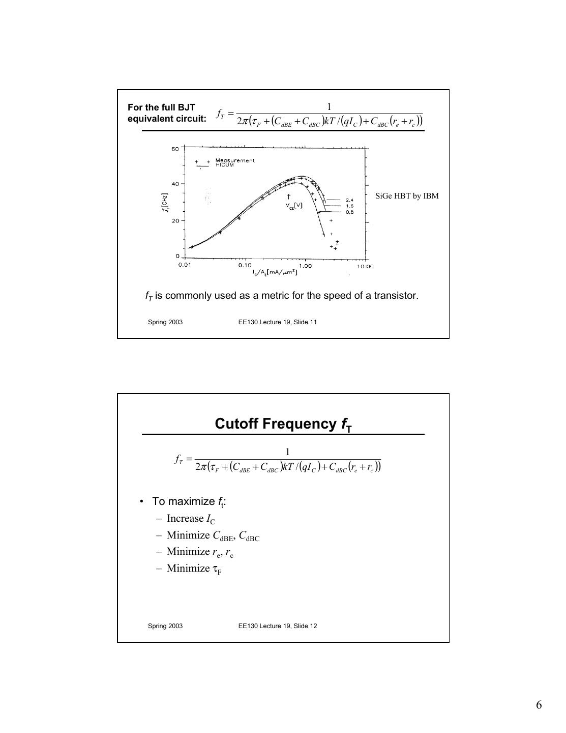
6 .For the full BJT 1 fT = equivalent circuit: 2π (τ F + (CdBE + CdBC )kT / (qI C ) + CdBC (re + rc )) SiGe HBT by IBM fT is commonly used as a metric for the speed of a transistor. Spring 2003 EE130 Lecture 19, Slide 11 Cutoff Frequency fT 1 fT = 2π (τ F + (CdBE + CdBC )kT / (qI C ) + CdBC (re + rc )) • To maximize ft: – Increase IC – Minimize CdBE, CdBC – Minimize re, rc – Minimize τF Spring 2003 EE130 Lecture 19, Slide 12 6
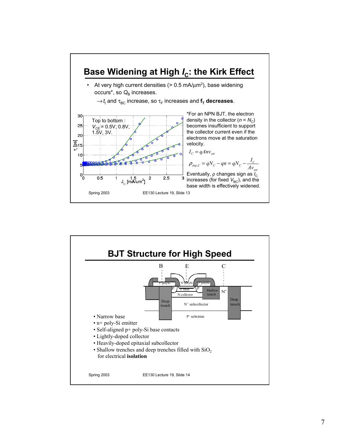
7 .Base Widening at High IC: the Kirk Effect • At very high current densities (> 0.5 mA/µm2), base widening occurs*, so QB increases. → tt and τBC increase, so τF increases and fT decreases. *For an NPN BJT, the electron Top to bottom : density in the collector (n = NC) VCE = 0.5V, 0.8V, becomes insufficient to support 1.5V, 3V. the collector current even if the electrons move at the saturation velocity. I C = qAnvsat IC ρ dep ,C = qN C − qn = qN C − Avsat Eventually, ρ changes sign as IC increases (for fixed VBC), and the base width is effectively widened. Spring 2003 EE130 Lecture 19, Slide 13 BJT Structure for High Speed B E C P+polySi N+ polySi P+polySi p+ P base p+ Shallow N+ N collector trench Deep Deep trench N+ subcollector trench • Narrow base P− substrate • n+ poly-Si emitter • Self-aligned p+ poly-Si base contacts • Lightly-doped collector • Heavily-doped epitaxial subcollector • Shallow trenches and deep trenches filled with SiO2 for electrical isolation Spring 2003 EE130 Lecture 19, Slide 14 7


