- 快召唤伙伴们来围观吧
- 微博 QQ QQ空间 贴吧
- 文档嵌入链接
- 复制
- 微信扫一扫分享
- 已成功复制到剪贴板
模拟集成电路
展开查看详情
1 .Chapter 10 Analog Integrated Circuits and its application Introduction The 741 Op-Amp Circuit The ideal Op Amp The inverting configuration The noninverting configuration Integrator and differentiator Other operation application
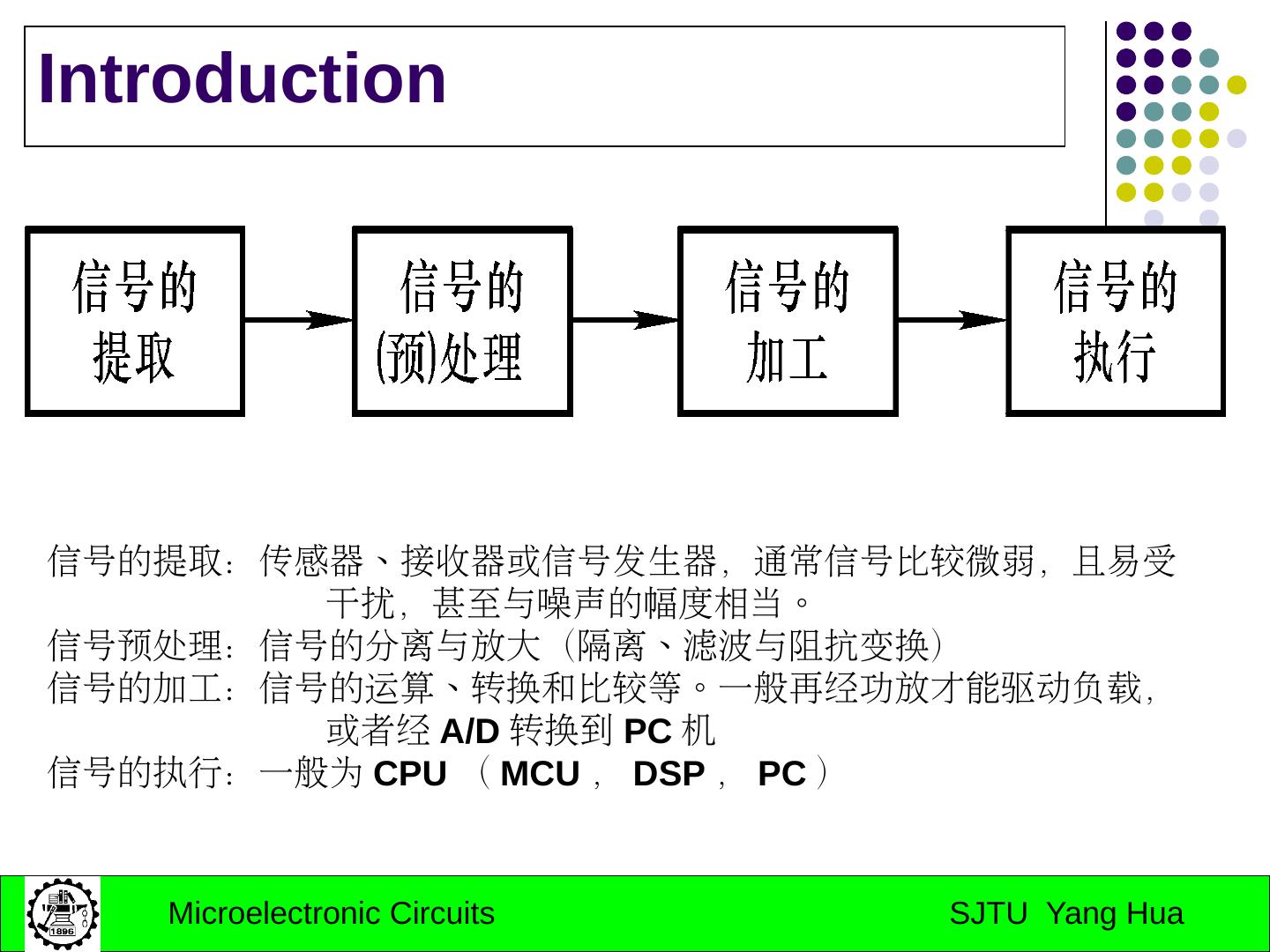
2 .Introduction 信号的提取:传感器、接收器或信号发生器,通常信号比较微弱,且易受 干扰,甚至与噪声的幅度相当。 信号预处理:信号的分离与放大(隔离、滤波与阻抗变换) 信号的加工:信号的运算、转换和比较等。一般再经功放才能驱动负载, 或者经 A/D 转换到 PC 机 信号的执行:一般为 CPU ( MCU , DSP , PC )
3 .Part 1. The 741 Op-Amp Circuit and analysis. Part 2. Analog integrated circuits’ application _ the application of operational amplifier _ the application of comparer circuits Content
4 .Part I: Analog ICs include operational amplifiers, analog multipliers, A/D converters, D/A converters, PLL, etc. A complete op amp is realized by combining analog circuit building blocks. The bipolar op-amp has the general purpose variety and is designed to fit a wide range of specifications. The terminal characteristics is nearly ideal.
5 .The 741 Op-Amp Circuit
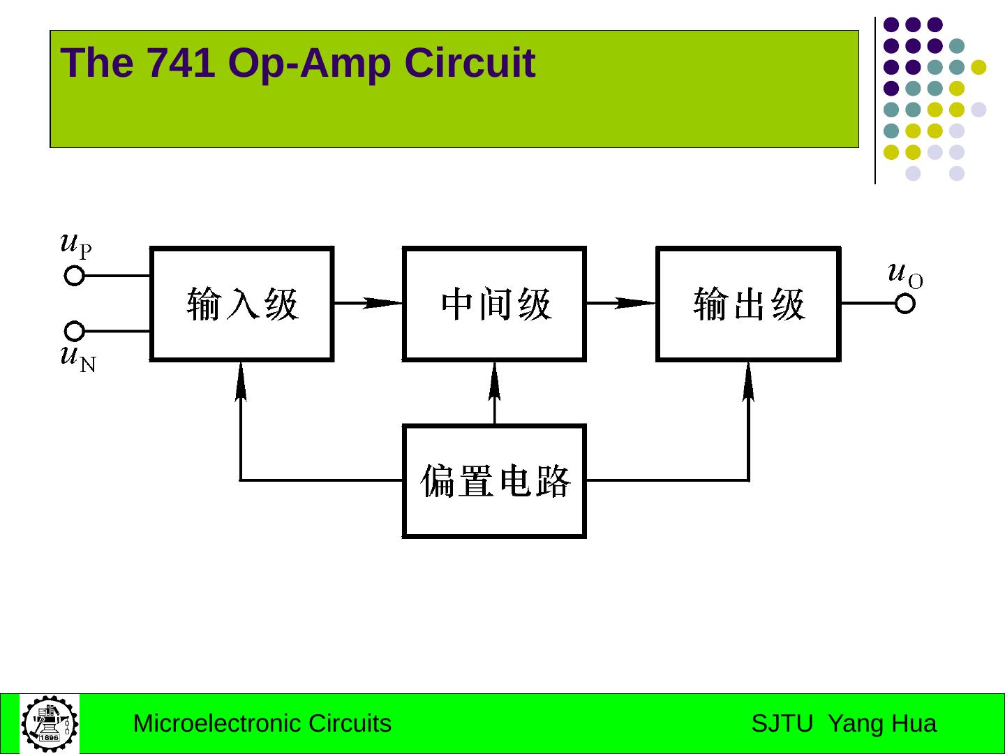
6 .Structure “ 化整为零”:划分偏置电路、输入级、中间级和输出级 “分析功能”:分别分析各部分的结构形式及特点 “统观整体” :研究各部分电路之间的联系 “定量估算”:必要时做定量分析
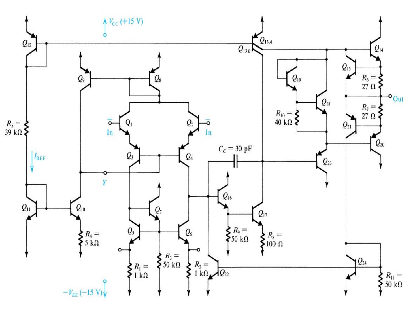
7 .General Description 24 transistors, few resistors and only one capacitor Two power supplies Short-circuit protection
8 .
9 .
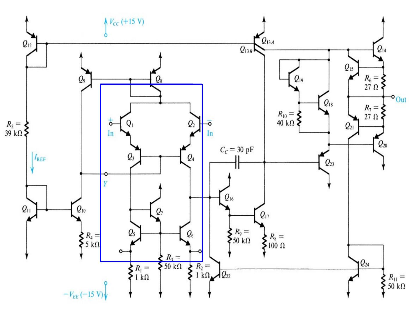
10 .The Input Stage The input stage consists of transistors Q1 through Q7. Q1-Q4 is the differential version of CC and CB configuration. High input resistance. Current source ( Q5-Q7 ) is the active load of input stage. It not only provides a high-resistance load but also converts the signal from differential to single-ended form with no loss in gain or common-mode rejection.
11 .The Intermediate Stage The intermediate stage is composed of Q 16 , Q 17 and Q 13B. Common-collector configuration for Q 16 gives this stage a high input resistance as well as reduces the load effect on the input stage. Common-emitter configuration for Q 17 provides high voltage gain because of the active load Q 13B. Capacitor Cc introduces the miller compensation to insure that the op amp has a very high unit-gain frequency.
12 .The Intermediate Stage The intermediate stage is composed of Q 16 , Q 17 and Q 13B. Common-collector configuration for Q 16 gives this stage a high input resistance as well as reduces the load effect on the input stage. Common-emitter configuration for Q 17 provides high voltage gain because of the active load Q 13B. Capacitor Cc introduces the miller compensation to insure that the op amp has a very high unit-gain frequency.
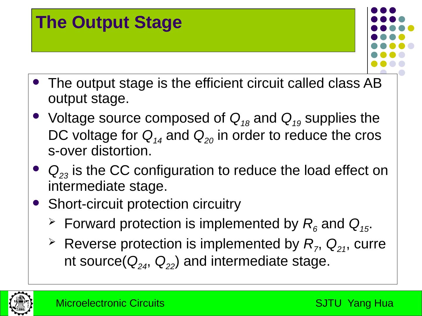
13 .The Output Stage The output stage is the efficient circuit called class AB output stage. Voltage source composed of Q 18 and Q 19 supplies the DC voltage for Q 14 and Q 20 in order to reduce the cross-over distortion. Q 23 is the CC configuration to reduce the load effect on intermediate stage. Short-circuit protection circuitry Forward protection is implemented by R 6 and Q 15 . Reverse protection is implemented by R 7 , Q 21 , current source( Q 24 , Q 22 ) and intermediate stage.
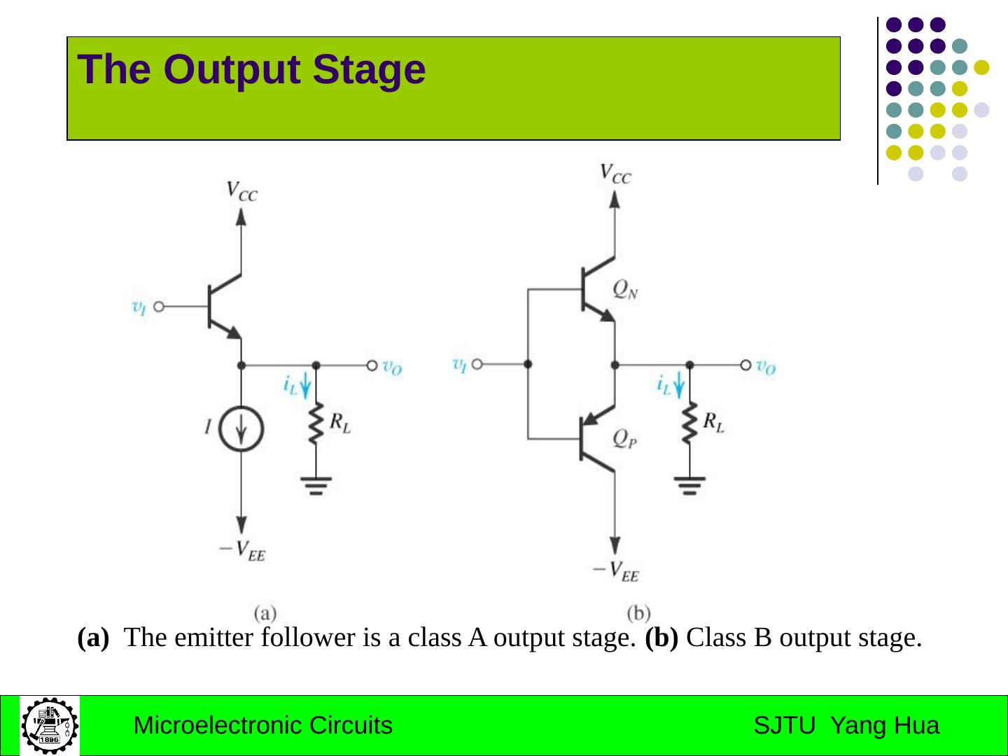
14 .The Output Stage (a) The emitter follower is a class A output stage. (b) Class B output stage.
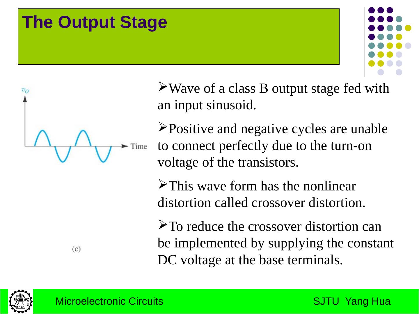
15 .The Output Stage Wave of a class B output stage fed with an input sinusoid. Positive and negative cycles are unable to connect perfectly due to the turn-on voltage of the transistors. This wave form has the nonlinear distortion called crossover distortion. To reduce the crossover distortion can be implemented by supplying the constant DC voltage at the base terminals.
16 .The Output Stage Q N and Q P provides the voltage drop which equals to the summer of turn-on voltages of Q N and Q P. This circuit is call Class AB output stage.
17 .The Output Stage Q N and Q P provides the voltage drop which equals to the summer of turn-on voltages of Q N and Q P. This circuit is call Class AB output stage.
18 .The Biasing Circuits Reference current is generated by Q 12 , Q 11 and R 5 . Wilder current provides biasing current in the order of μA . Double-collector transistor is similar to the two-output current mirror. Q 13B provides biasing current for intermediate stage, Q 13A for output stage. Q 5 , Q 6 and Q 7 is composed of the current source to be an active load for input stage.
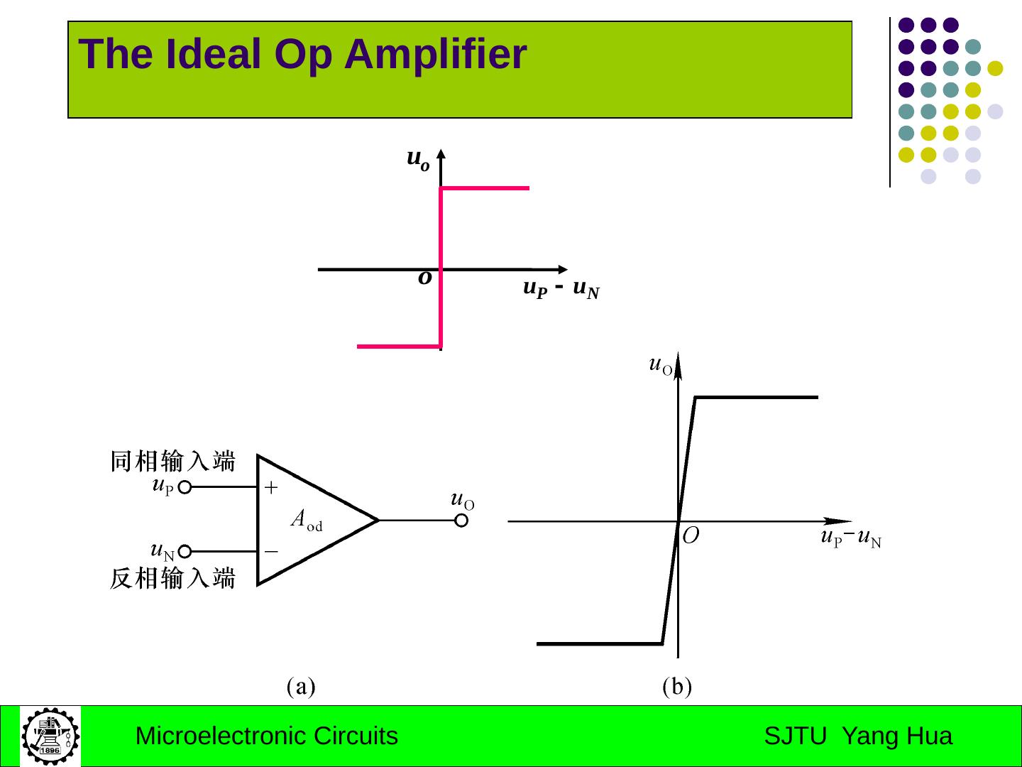
19 .The Ideal Op Amplifier symbol for the op amp
20 .The Ideal Op Amplifier The op amp shown connected to dc power supplies.
21 .Characteristics of the Ideal Op Amplifier Differential input resistance is infinite. Differential voltage gain is infinite. CMRR is infinite. Bandwidth is infinite. Output resistance is zero. Offset voltage and current is zero . No difference voltage between inverting and noninverting terminals. No input currents.
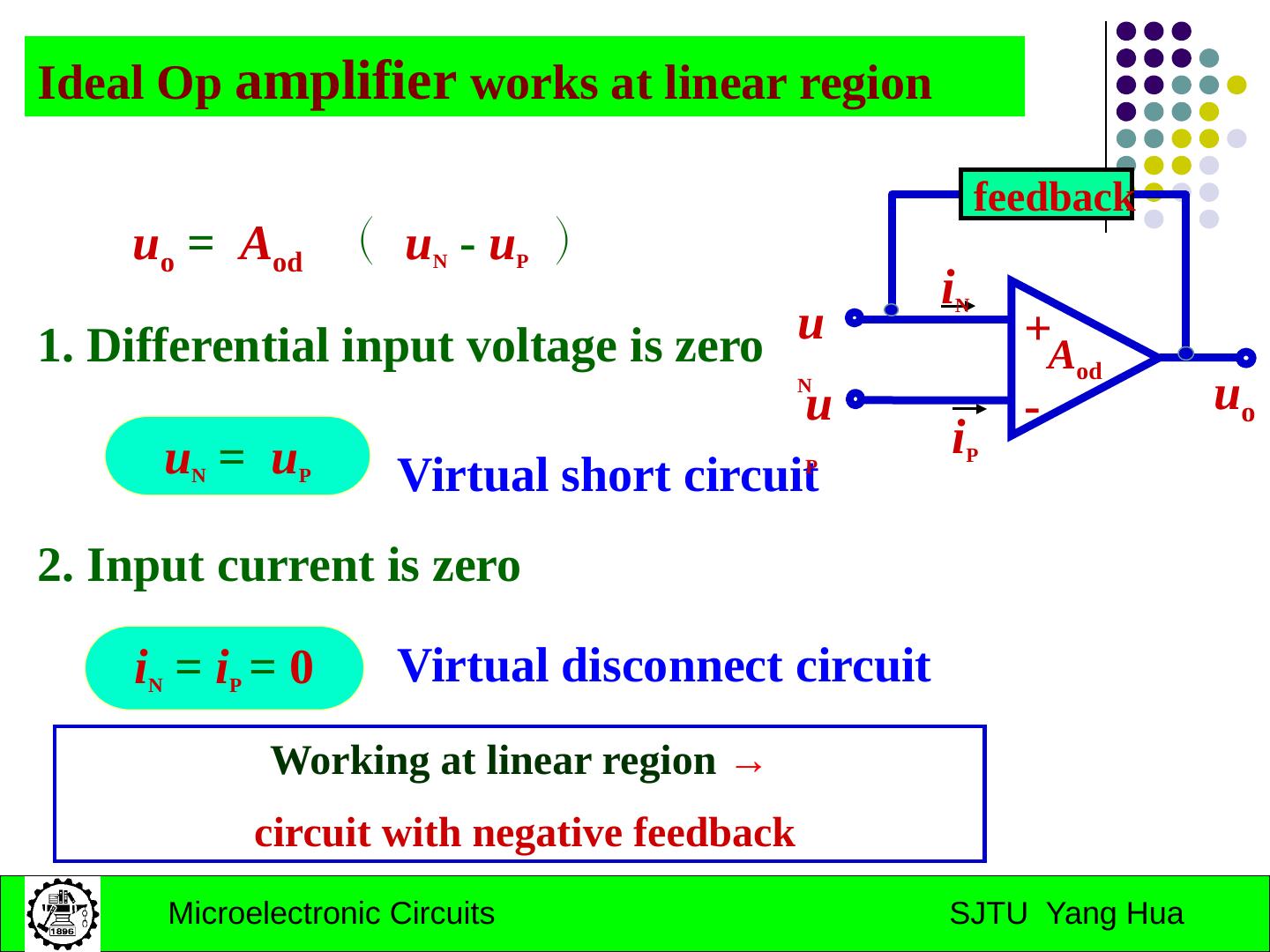
22 .i N = i P = 0 u N = u P 1. Differential input voltage is zero 2. Input current is zero u o = A od ( u N - u P ) Virtual short circuit Virtual disconnect circuit A od + - u N u P u o i N i P feedback Working at linear region → circuit with negative feedback Ideal Op amplifier works at linear region
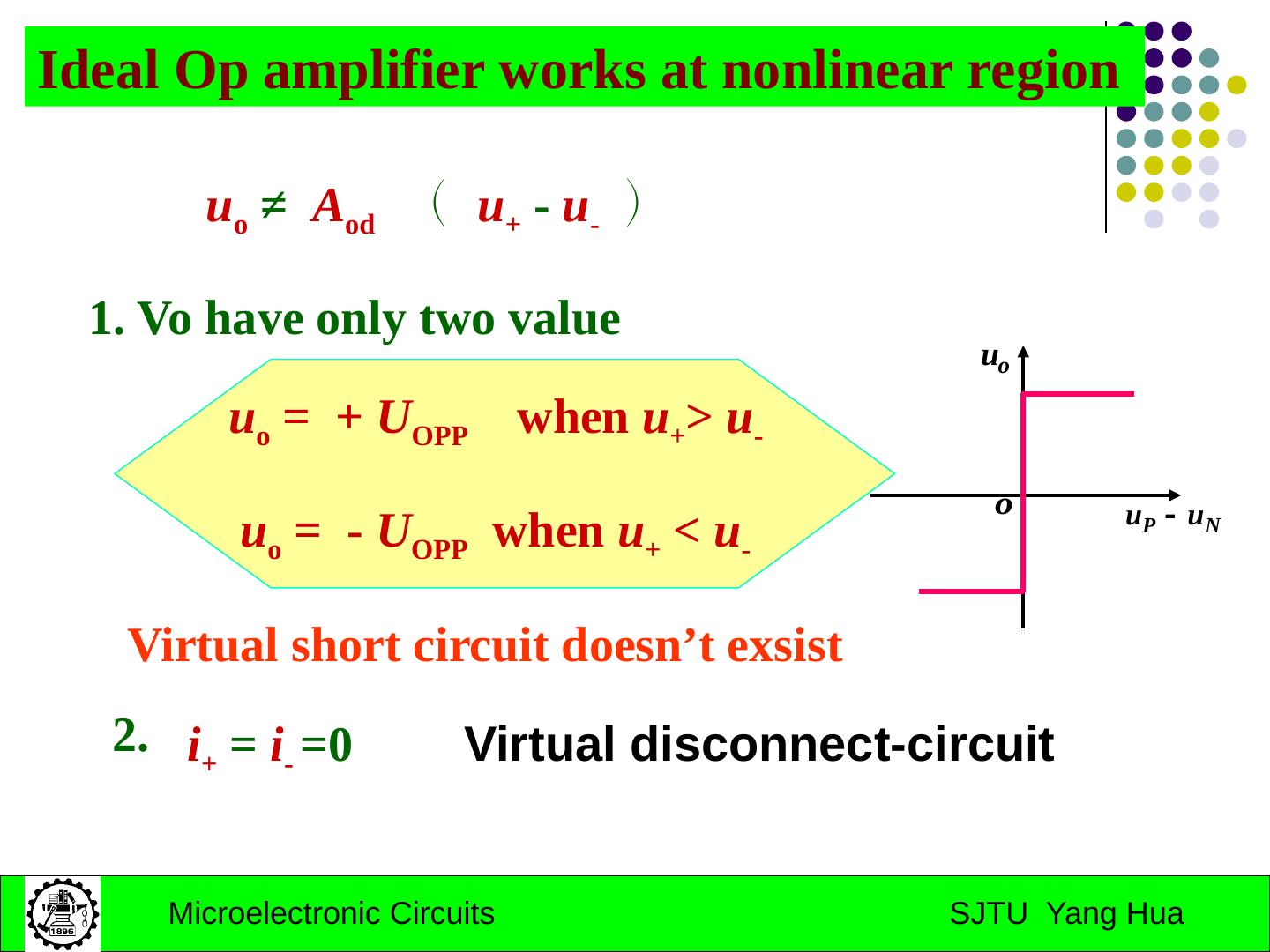
23 .Ideal Op amplifier works at nonlinear region u o ≠ A od ( u + - u - ) u o = + U OPP when u + > u - u o = - U OPP when u + < u - 1. Vo have only two value 2. i + = i - =0 Virtual disconnect-circuit Virtual short circuit doesn’t exsist
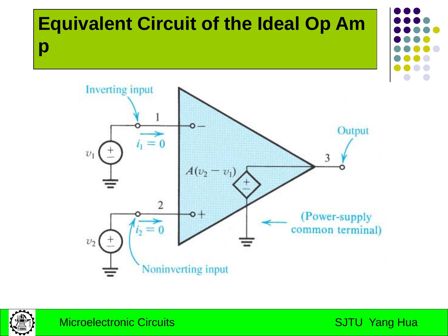
24 .Equivalent Circuit of the Ideal Op Amp
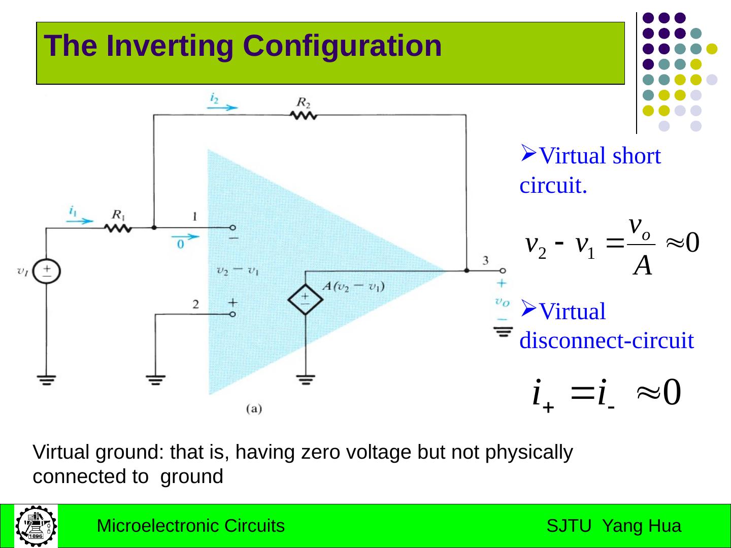
25 .The Inverting Configuration Virtual short circuit . Virtual ground: that is, having zero voltage but not physically connected to ground Virtual disconnect-circuit
26 .The Inverting Configuration The inverting closed-loop configuration.
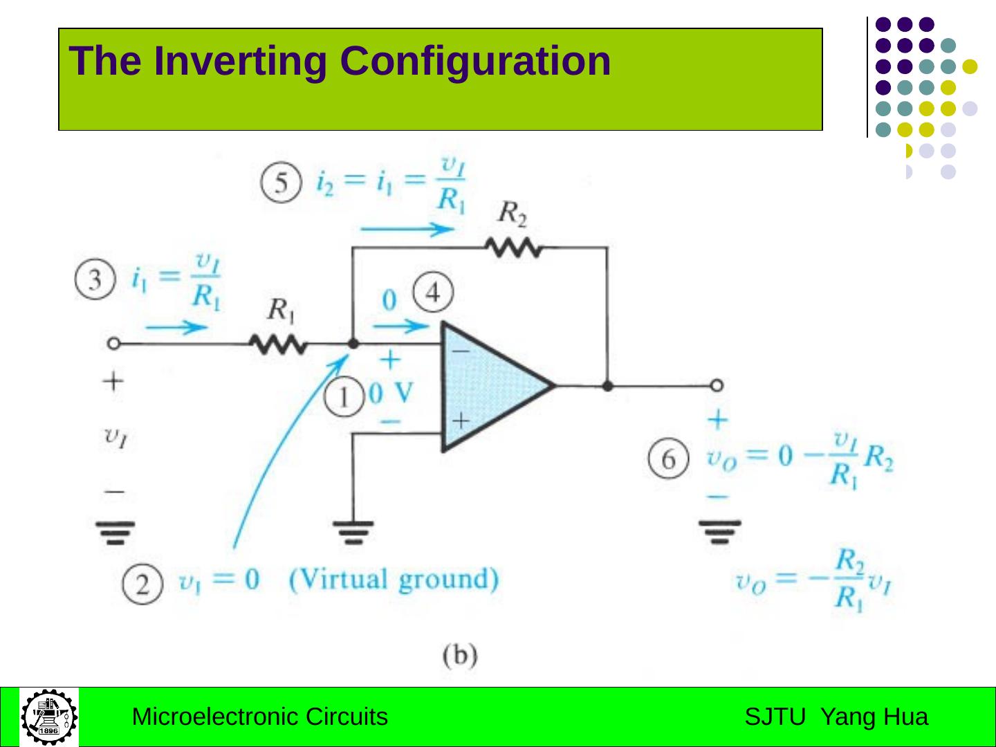
27 .The Inverting Configuration
28 .Effect of finite open-loop gain
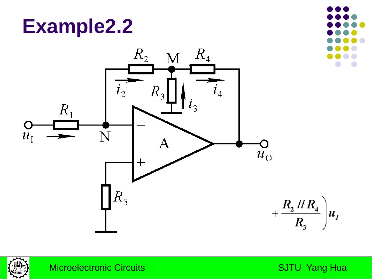
29 .The Inverting Configuration Shunt-shunt negative feedback Closed-loop gain depends entirely on passive components and is independent of the op amplifier. Engineer can make the closed-loop gain as accurate as he wants as long as the passive components are accurate. Exercises: example 2.2


